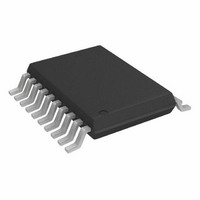
AD5445YRUZ Analog Devices Inc, AD5445YRUZ Datasheet - Page 3

AD5445YRUZ
Manufacturer Part Number
AD5445YRUZ
Description
IC DAC 12BIT PARALL IOUT 20TSSOP
Manufacturer
Analog Devices Inc
Datasheet
1.AD5445YRUZ.pdf
(32 pages)
Specifications of AD5445YRUZ
Data Interface
Parallel
Settling Time
80ns
Number Of Bits
12
Number Of Converters
1
Voltage Supply Source
Single Supply
Power Dissipation (max)
25µW
Operating Temperature
-40°C ~ 125°C
Mounting Type
Surface Mount
Package / Case
20-TSSOP
Resolution (bits)
12bit
Sampling Rate
20.4MSPS
Input Channel Type
Parallel
Supply Voltage Range - Analog
2.5V To 5.5V
Supply Current
400nA
Digital Ic Case Style
TSSOP
Number Of Channels
1
Resolution
12b
Conversion Rate
20.4MSPS
Interface Type
Parallel
Single Supply Voltage (typ)
3.3/5V
Dual Supply Voltage (typ)
Not RequiredV
Architecture
R-2R
Power Supply Requirement
Single
Output Type
Current
Integral Nonlinearity Error
±1+/- LSB
Single Supply Voltage (min)
2.5V
Single Supply Voltage (max)
5.5V
Dual Supply Voltage (min)
Not RequiredV
Dual Supply Voltage (max)
Not RequiredV
Operating Temp Range
-40C to 125C
Operating Temperature Classification
Automotive
Mounting
Surface Mount
Pin Count
20
Package Type
TSSOP
Lead Free Status / RoHS Status
Lead free / RoHS Compliant
For Use With
EVAL-AD5445EBZ - BOARD EVALUATION FOR AD5445
Lead Free Status / Rohs Status
Compliant
Available stocks
Company
Part Number
Manufacturer
Quantity
Price
Part Number:
AD5445YRUZ
Manufacturer:
ADI/亚德诺
Quantity:
20 000
SPECIFICATIONS
V
otherwise noted. DC performance measured with OP177and ac performance measured with AD8038, unless otherwise noted.
Table 1.
Parameter
STATIC PERFORMANCE
REFERENCE INPUT
DIGITAL INPUTS/OUTPUT
DYNAMIC PERFORMANCE
DD
AD5424
AD5433
AD5445
Gain Error
Gain Error Temperature Coefficient
Output Leakage Current
Reference Input Range
V
R
Input Capacitance
Input High Voltage, V
Input Low Voltage, V
Output High Voltage, V
Output Low Voltage, V
Input Leakage Current, I
Input Capacitance
Reference Multiplying Bandwidth
Output Voltage Settling Time
Digital Delay
10% to 90% Settling Time
Digital-to-Analog Glitch Impulse
Multiplying Feedthrough Error
REF
FB
= 2.5 V to 5.5 V, V
Resolution
Relative Accuracy
Differential Nonlinearity
Resolution
Relative Accuracy
Differential Nonlinearity
Resolution
Relative Accuracy
Differential Nonlinearity
Code Zero Scale
Code Full Scale
Measured to ±16 mV of full scale
Measured to ±4 mV of full scale
Measured to ±1 mV of full scale
Resistance
Input Resistance
1
IL
REF
IH
OL
1
OH
1
= 10 V, I
IL
1
OUT
1
2 = 0 V. Temperature range for Y version: −40°C to +125°C. All specifications T
Min
8
8
1.7
V
V
DD
DD
− 1
− 0.5
Typ
±5
±10
10
10
3
5
4
10
30
35
80
20
15
2
70
48
Max
8
±0.25
±0.5
10
±0.5
±1
12
±1
–1/+2
±10
±10
±20
12
12
6
8
0.6
0.4
0.4
1
10
40
30
Rev. B | Page 3 of 32
60
70
120
Unit
Bits
LSB
LSB
Bits
LSB
LSB
Bits
LSB
LSB
mV
ppm FSR/°C
nA
nA
V
kΩ
kΩ
pF
pF
V
V
V
V
V
V
μA
pF
MHz
ns
ns
ns
ns
ns
nV-s
dB
dB
Conditions
Guaranteed monotonic
Guaranteed monotonic
Guaranteed monotonic
Data = 0×0000, T
Data = 0×0000, T = −40°C to +125°C, I
Input resistance TC = –50 ppm/°C
Input resistance TC = –50 ppm/°C
V
V
V
V
V
V
alternately loaded with 0s and 1s
Interface delay time
Rise and fall time, V
1 LSB change around major carry, V
DAC latch loaded with all 0s, V
Reference = 1 MHz
Reference = 10 MHz
DD
DD
DD
DD
REF
REF
= 4.5 V to 5 V, I
= 2.5 V to 3.6 V, I
= 4.5 V to 5 V, I
= 2.5 V to 3.6 V, I
= ±3.5 V; DAC loaded all 1s
= ±3.5 V, R
AD5424/AD5433/AD5445
LOAD
A
SOURCE
SINK
= 25°C, I
= 100 Ω, DAC latch
REF
SOURCE
SINK
= 200 μA
= 10 V, R
= 200 μA
= 200 μA
MIN
= 200 μA
OUT
to T
1
REF
LOAD
= ±3.5 V
MAX
= 100 Ω
REF
, unless
OUT
= 0 V
1


