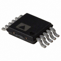
AD5305BRMZ Analog Devices Inc, AD5305BRMZ Datasheet

AD5305BRMZ
Specifications of AD5305BRMZ
Available stocks
Related parts for AD5305BRMZ
AD5305BRMZ Summary of contents
Page 1
FEATURES AD5305: 4 buffered 8-bit DACs in 10-lead MSOP A version: ±1 LSB INL, B version: ±0.625 LSB INL AD5315: 4 buffered 10-bit DACs in 10-lead MSOP A version: ±4 LSB INL, B version: ±2.5 LSB INL AD5325: 4 buffered ...
Page 2
AD5305/AD5315/AD5325 TABLE OF CONTENTS Features .............................................................................................. 1 Applications....................................................................................... 1 General Description ......................................................................... 1 Functional Block Diagram .............................................................. 1 Revision History ............................................................................... 2 Specifications..................................................................................... 3 AC Characteristics........................................................................ 5 Timing Characteristics ................................................................ 5 Absolute Maximum Ratings............................................................ 7 ESD Caution.................................................................................. 7 Pin Configuration ...
Page 3
SPECIFICATIONS kΩ to GND REF L Table 1. Parameter 2 Min PERFORMANCE AD5305 Resolution Relative Accuracy Differential Nonlinearity AD5315 Resolution Relative ...
Page 4
AD5305/AD5315/AD5325 2 Parameter Min 5 LOGIC INPUTS (A0) Input Current Input Low Voltage Input High Voltage, V 2.4 IH 2.1 2.0 Pin Capacitance 5 LOGIC INPUTS (SCL, SDA) Input High Voltage Input Low ...
Page 5
AC CHARACTERISTICS kΩ to GND Table 2. Parameter 2, 3 Output Voltage Settling Time AD5305 AD5315 AD5325 Slew Rate Major-Code Transition Glitch Energy Digital Feedthrough Digital Crosstalk ...
Page 6
AD5305/AD5315/AD5325 SDA SCL t 4 START CONDITION Figure 2. 2-Wire Serial Interface Timing Diagram Rev Page ...
Page 7
ABSOLUTE MAXIMUM RATINGS T = 25°C, unless otherwise noted. A Table 4. 1 Parameter Rating V to GND –0 SCL, SDA to GND –0 GND –0 Reference ...
Page 8
AD5305/AD5315/AD5325 PIN CONFIGURATION AND FUNCTION DESCRIPTIONS Table 5. Pin Function Descriptions Pin No. Mnemonic Description 1 V Power Supply Input. These parts can be operated from 2 5.5 V and the supply should be decoupled to GND. DD ...
Page 9
TYPICAL PERFORMANCE CHARACTERISTICS 1 25° 0.5 0 –0.5 –1 100 150 CODE Figure 4. AD5305 Typical INL Plot 25° –1 ...
Page 10
AD5305/AD5315/AD5325 0. 25°C A 0.25 MAXINL 0 MIN DNL –0.25 MIN INL –0. (V) REF Figure 10. AD5305 INL and DNL Error vs ...
Page 11
V (V) DD Figure 16. Supply Current vs. Supply Voltage 0.5 0.4 0.3 –40°C 0.2 +25°C 0.1 +105°C 0 2.5 3.0 3.5 4.0 4.5 V ...
Page 12
AD5305/AD5315/AD5325 300 350 400 450 500 I (µA) DD Figure 22. I Histogram with and 2.50 2.49 2.48 2.47 1µs/DIV Figure 23. AD5325 Major-Code Transition Glitch Energy 10 0 ...
Page 13
TERMINOLOGY Relative Accuracy For the DAC, relative accuracy or integral nonlinearity (INL measure of the maximum deviation, in LSB, from a straight line passing through the endpoints of the DAC transfer function. Typical INL versus code plots can ...
Page 14
AD5305/AD5315/AD5325 OUTPUT IDEAL VOLTAGE ACTUAL NEGATIVE OFFSET DAC CODE ERROR DEAD BAND CODES AMPLIFIER FOOTROOM (1mV) NEGATIVE OFFSET ERROR Figure 27. Transfer Function with Negative Offset GAIN ERROR PLUS OFFSET ERROR OUTPUT VOLTAGE POSITIVE OFFSET Rev Page 14 ...
Page 15
FUNCTIONAL DESCRIPTION The AD5305/AD5315/AD5325 are quad resistor-string DACs fabricated on a CMOS process with resolutions of 8, 10, and 12 bits, respectively. Each contains four output buffer amplifiers and is written to via a 2-wire serial interface. They operate from ...
Page 16
AD5305/AD5315/AD5325 SERIAL INTERFACE The AD5305/AD5315/AD5325 are controlled via an I compatible serial bus. The DACs are connected to this bus as slave devices (that is, no clock is generated by the AD5305/ AD5315/AD5325 DACs). This interface is SMBus compatible at ...
Page 17
Table 7. CLR and LDAC Bit Descriptions Bit Description CLR [0] All DAC registers and input registers are filled with 0s on completion of the write sequence. [1] Normal operation. LDAC [0] All four DAC registers and, therefore, all DAC ...
Page 18
AD5305/AD5315/AD5325 SCL SDA START COND ADDRESS BYTE BY MASTER SCL SDA REPEATED START ADDRESS BYTE COND BY MASTER SCL MSB SDA LEAST SIGNIFICANT DATA BYTE NOTE: DATA BYTES ARE THE SAME AS ...
Page 19
When both bits are set to 0, the DAC works normally with its normal power consumption of 600 μ However, for the three power-down modes, the supply current falls to 200 (80 nA ...
Page 20
AD5305/AD5315/AD5325 APPLICATIONS TYPICAL APPLICATION CIRCUIT The AD5305/AD5315/AD5325 can be used with a wide range of reference voltages where the devices offer full, one-quadrant multiplying capability over a reference range More typically, these devices are used ...
Page 21
AD5305/AD5315/AD5325 AS A DIGITALLY PROGRAMMABLE WINDOW DETECTOR A digitally programmable upper/lower limit detector using two of the DACs in the AD5305/AD5315/AD5325 is shown in Figure 39. The upper and lower limits for the test are loaded to DAC A and ...
Page 22
AD5305/AD5315/AD5325 Table 9. Overview of All AD53xx Serial Devices Part No. Resolution No. of DACs SINGLES AD5300 8 1 AD5310 10 1 AD5320 12 1 AD5301 8 1 AD5311 10 1 AD5321 12 1 DUALS AD5302 8 2 AD5312 10 ...
Page 23
... AD5305BRM −40°C to +105°C AD5305BRM-REEL −40°C to +105°C AD5305BRM-REEL7 −40°C to +105°C 1 AD5305BRMZ −40°C to +105°C AD5305BRMZ-REEL7 1 −40°C to +105°C AD5315ARM −40°C to +105°C AD5315ARM-REEL7 −40°C to +105°C 1 AD5315ARMZ −40°C to +105°C AD5315BRM − ...
Page 24
AD5305/AD5315/AD5325 NOTES Purchase of licensed components of Analog Devices or one of its sublicensed Associated Companies conveys a license for the purchaser under the Philips I 2 Rights to use these components system, ...


