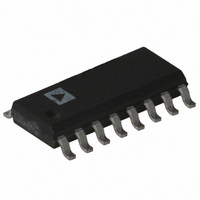
AD7524JRZ Analog Devices Inc, AD7524JRZ Datasheet - Page 4

AD7524JRZ
Manufacturer Part Number
AD7524JRZ
Description
IC DAC 8BIT MULTIPLYING 16-SOIC
Manufacturer
Analog Devices Inc
Datasheet
1.AD7524JNZ.pdf
(8 pages)
Specifications of AD7524JRZ
Data Interface
Parallel
Settling Time
250ns
Number Of Bits
8
Number Of Converters
1
Voltage Supply Source
Single Supply
Power Dissipation (max)
30mW
Operating Temperature
-40°C ~ 85°C
Mounting Type
Surface Mount
Package / Case
16-SOIC (3.9mm Width)
Resolution (bits)
8bit
Sampling Rate
4MSPS
Input Channel Type
Parallel
Supply Current
2mA
Digital Ic Case Style
SOIC
No. Of Pins
16
Lead Free Status / RoHS Status
Lead free / RoHS Compliant
Available stocks
Company
Part Number
Manufacturer
Quantity
Price
Part Number:
AD7524JRZ
Manufacturer:
ADI/亚德诺
Quantity:
20 000
Part Number:
AD7524JRZ-REEL
Manufacturer:
ADI/亚德诺
Quantity:
20 000
Company:
Part Number:
AD7524JRZ-REEL7
Manufacturer:
MOT
Quantity:
225
Part Number:
AD7524JRZ-REEL7
Manufacturer:
ADI/亚德诺
Quantity:
20 000
AD7524
CIRCUIT DESCRIPTION
CIRCUIT INFORMATION
The AD7524, an 8-bit multiplying D/A converter, consists of a
highly stable thin film R-2R ladder and eight N-channel current
switches on a monolithic chip. Most applications require the
addition of only an output operational amplifier and a voltage
or current reference.
The simplified D/A circuit is shown in Figure 1. An inverted
R-2R ladder structure is used—that is, the binarily weighted
currents are switched between the OUT1 and OUT2 bus lines,
thus maintaining a constant current in each ladder leg indepen-
dent of the switch state.
EQUIVALENT CIRCUIT ANALYSIS
The equivalent circuit for all digital inputs LOW is shown in
Figures 2. In Figure 2 with all digital inputs LOW, the refer-
ence current is switched to OUT2. The current source I
is composed of surface and junction leakages to the substrate
while the
rent drain through the termination resistor on the R-2R ladder.
The “ON” capacitance of the output N-channel switches is
120 pF, as shown on the OUT2 terminal. The “OFF” switch
capacitance is 30 pF, as shown on the OUT1 terminal. Analysis
of the circuit for all digital inputs high is similar to Figure 2
however, the “ON” switches are now on terminal OUT1, hence
the 120 pF appears at that terminal.
INTERFACE LOGIC INFORMATION
MODE SELECTION
AD7524 mode selection is controlled by the CS and WR inputs.
Figure 2. AD7524 DAC Equivalent Circuit—All Digital
Inputs Low
256
1
Figure 1. Functional Diagram
current source represents a constant 1-bit cur-
LEAKAGE
–4–
WRITE MODE
When CS and WR are both LOW, the AD7524 is in the
WRITE mode, and the AD7524 analog output responds to data
activity at the DB0–DB7 data bus inputs. In this mode, the
AD7524 acts like a nonlatched input D/A converter.
HOLD MODE
When either CS or WR is HIGH, the AD7524 is in the HOLD
mode. The AD7524 analog output holds the value correspond-
ing to the last digital input present at DB0–DB7 prior to WR or
CS assuming the HIGH state.
CS
L
H
X
L = Low State, H = High State, X = Don't Care.
WRITE CYCLE TIMING DIAGRAM
Typical plots of supply current, I
V
IN
, for V
DD
WR
L
X
H
Figure 3. Supply Current vs. Logic Level
= +5 V and V
MODE SELECTION TABLE
Mode
Write
Hold
Hold
DD
= +15 V are shown above.
DD
DAC Response
DAC responds to data bus
(DB0–DB7) inputs.
Data bus (DB0–DB7) is
Locked Out:
DAC holds last data present
when WR or CS assumed
HIGH state.
, versus logic input voltage,
REV. B


