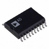
AD7392ARZ Analog Devices Inc, AD7392ARZ Datasheet

AD7392ARZ
Specifications of AD7392ARZ
Available stocks
Related parts for AD7392ARZ
AD7392ARZ Summary of contents
Page 1
FEATURES Micropower: 100 μA 0.1 μA typical power shutdown Single-supply 2 5.5 V operation AD7392: 12-bit resolution AD7393: 10-bit resolution 0.9 LSB differential nonlinearity error APPLICATIONS Automotive 0 4.5 V output span voltage Portable communications Digitally ...
Page 2
AD7392/AD7393 TABLE OF CONTENTS Features .............................................................................................. 1 Applications....................................................................................... 1 Functional Block Diagram .............................................................. 1 General Description ......................................................................... 1 Revision History ............................................................................... 2 Specifications..................................................................................... 3 Electrical Characteristics............................................................. 3 Timing Diagram ........................................................................... 5 Absolute Maximum Ratings............................................................ 6 ESD Caution.................................................................................. 6 Pin Configurations ...
Page 3
SPECIFICATIONS ELECTRICAL CHARACTERISTICS 2.5 V, −40°C < T < +85°C, unless otherwise noted. REF A Table 1. AD7392 Parameter STATIC PERFORMANCE 1 Resolution 2 Relative Accuracy 2 Differential Nonlinearity Zero-Scale Error Full-Scale Voltage Error Full-Scale Temperature Coefficient ...
Page 4
AD7392/AD7393 2.5 V, −40°C < T < +85°C, unless otherwise noted. REF A Table 2. AD7393 Parameter STATIC PERFORMANCE 1 Resolution 2 Relative Accuracy 2 Differential Nonlinearity Zero-Scale Error Full-Scale Voltage Error Full-Scale Temperature Coefficient 3 REFERENCE ...
Page 5
TIMING DIAGRAM D11 DATA VALID ±0.1%FS OUT ERROR BAND Figure 2. Timing Diagram Rev Page 5 of ...
Page 6
AD7392/AD7393 ABSOLUTE MAXIMUM RATINGS Table 3. Parameter V to GND GND REF Logic Inputs to GND V to GND OUT I Short Circuit to GND OUT DGND to AGND Package Power Dissipation Thermal Resistance (θ ...
Page 7
PIN CONFIGURATIONS AND FUNCTION DESCRIPTIONS SHDN AD7392 D0 5 TOP VIEW D1 6 (Not to Scale Figure 3. AD7392 Pin Configuration Table 4. AD7392 ...
Page 8
AD7392/AD7393 TYPICAL PERFORMANCE CHARACTERISTICS 1.0 AD7392 0.8 0.6 0.4 0.2 0 –0.2 –0.4 –0.6 –0.8 –1.0 0 512 1024 1536 2048 CODE (Decimal) Figure 5. AD7392 Integral Nonlinearity Error vs. Code 1.0 AD7393 0.8 0.6 0.4 0.2 0 –0.2 –0.4 ...
Page 9
AD7392 25° LOGIC FROM LOGIC 0.5 1.0 1.5 2.0 V (V) IN Figure ...
Page 10
AD7392/AD7393 2µs V OUT (5mV/DIV) CS (5V/DIV) 20mV TIME (2µs/DIV) Figure 17. Midscale Transition Performance 5µs V OUT (5mV/DIV) 5mV TIME (5µs/DIV) Figure 18. Digital Feedthrough 100µs V OUT (1V/DIV) CS (5V/DIV) 1V TIME (100µs/DIV) Figure 19. Large Signal Settling ...
Page 11
AD7392 5V 500mV 100 100 (µ 2.5V REF CODE = 0xFFF 1MΩ TO GND 25°C V (V) A OUT SHDN ...
Page 12
AD7392/AD7393 THEORY OF OPERATION The AD7392/AD7393 comprise a set of pin-compatible, 12-/10- bit digital-to-analog converters (DACs). These single-supply operation devices consume less than 100 μA of current while operating from 2 5.5 V power supplies, making them ideal ...
Page 13
POWER SUPPLY The very low power consumption of the AD7392/AD7393 is a direct result of a circuit design that optimizes the CBCMOS process. By using the low power characteristics of CMOS for the logic and the low noise, tight-matching of ...
Page 14
AD7392/AD7393 RESET PIN (RS) Forcing the asynchronous RS pin low sets the DAC register to all 0s, so the DAC output voltage The reset function is useful for setting the DAC outputs power-up or ...
Page 15
BIPOLAR OUTPUT OPERATION Although the AD7393 is designed for single-supply operation, the output can be easily configured for bipolar operation. A typical circuit is shown in Figure 33. This circuit uses a clean, regulated 5 V supply for power, which ...
Page 16
AD7392/AD7393 OUTLINE DIMENSIONS 0.210 (5.33) MAX 0.150 (3.81) 0.130 (3.30) 0.115 (2.92) 0.022 (0.56) 0.018 (0.46) 0.014 (0.36) 0.30 (0.0118) 0.10 (0.0039) COPLANARITY 0.10 1.060 (26.92) 1.030 (26.16) 0.980 (24.89 0.280 (7.11) 0.250 (6.35) 1 0.240 (6.10) 10 ...
Page 17
... ORDERING GUIDE Model Resolution (Bits) AD7392AN 12 1 AD7392ANZ 12 AD7392AR 12 AD7392AR-REEL 12 AD7392ARZ AD7392ARZ-REEL 12 AD7393AN 10 AD7393AR 10 1 AD7393ARZ RoHS Compliant Part. Temperature Range Package Description −40°C to +85°C 20-Lead PDIP −40°C to +85°C 20-Lead PDIP −40°C to +85°C 20-Lead SOIC_W − ...
Page 18
AD7392/AD7393 NOTES Rev Page ...
Page 19
NOTES Rev Page AD7392/AD7393 ...
Page 20
AD7392/AD7393 NOTES ©1996–2007 Analog Devices, Inc. All rights reserved. Trademarks and registered trademarks are the property of their respective owners. C01121-0-8/07(C) Rev Page ...


