AD7528KNZ Analog Devices Inc, AD7528KNZ Datasheet - Page 3
AD7528KNZ
Manufacturer Part Number
AD7528KNZ
Description
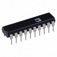
IC DAC 8BIT DUAL MULTIPLY 20-DIP
Manufacturer
Analog Devices Inc
Datasheet
1.AD7528KNZ.pdf
(8 pages)
Specifications of AD7528KNZ
Settling Time
400ns
Number Of Bits
8
Number Of Converters
2
Voltage Supply Source
Single Supply
Power Dissipation (max)
450mW
Operating Temperature
-40°C ~ 85°C
Mounting Type
Through Hole
Package / Case
20-DIP (0.300", 7.62mm)
Resolution (bits)
8bit
Sampling Rate
5.6MSPS
Input Channel Type
Parallel
Supply Current
2mA
Digital Ic Case Style
DIP
No. Of Pins
20
Data Interface
CMOS, Parallel, TTL
Lead Free Status / RoHS Status
Lead free / RoHS Compliant
Available stocks
Company
Part Number
Manufacturer
Quantity
Price
Company:

Part Number:
AD7528KNZ
Manufacturer:
MOT
Quantity:
6 225


REV. B
Parameter
CHANNEL-TO-CHANNEL ISOLATION
DIGITAL CROSSTALK
HARMONIC DISTORTlON
NOTES
1
2
3
4
5
6
Specifications subject to change without notice.
ABSOLUTE MAXIMUM RATINGS
(T
V
V
AGND to DGND . . . . . . . . . . . . . . . . . . . . . . . . V
DGND to AGND . . . . . . . . . . . . . . . . . . . . . . . . V
Digital Input Voltage to DGND . . . . . . . –0.3 V, V
V
V
V
Power Dissipation (Any Package) to +75 C . . . . . . . 450 mW
Operating Temperature Range
Storage Temperature . . . . . . . . . . . . . . . . . . –65 C to +150 C
Lead Temperature (Soldering, 10 secs) . . . . . . . . . . . . +300 C
CAUTION:
1. ESD sensitive device. The digital control inputs are diode
2. Do not insert this device into powered sockets. Remove
TERMINOLOGY
Relative Accuracy
Relative accuracy or endpoint nonlinearity is a measure of the
maximum deviation from a straight line passing through the
endpoints of the DAC transfer function. It is measured after
adjusting for zero and full scale and is normally expressed in
LSBs or as a percentage of full scale reading.
Differential Nonlinearity
Differential nonlinearity is the difference between the measured
change and the ideal 1 LSB change between any two adjacent
codes. A specified differential nonlinearity of 1 LSB max over
the operating temperature range ensures monotonicity.
Gain Error
Gain error or full-scale error is a measure of the output error
between an ideal DAC and the actual device output. For the
Temperature Ranges are J, K, L Versions: –40 C to +85 C
Specifications applies to both DACs in AD7528.
Guaranteed by design but not production tested.
Logic inputs are MOS Gates. Typical input current (+25 C) is less than 1 nA.
These characteristics are for design guidance only and are not subject to test.
Feedthrough can be further reduced by connecting the metal lid on the ceramic package
(suffix D) to DGND.
DD
DD
PIN2
REF
RFB
A
V
V
Derates above +75 C by . . . . . . . . . . . . . . . . . . . 6 mW/ C
Commercial (J, K, L) Grades . . . . . . . . . . . –40 C to +85 C
Industrial (A, B, C) Grades . . . . . . . . . . . . –40 C to +85 C
Extended (S, T, U) Grades . . . . . . . . . . . –55 C to +125 C
protected; however, permanent damage may occur on uncon-
nected devices subjected to high energy electrostatic fields.
Unused devices must be stored in conductive foam or shunts.
power before insertion or removal.
REF
REF
= +25 C unless otherwise noted)
to AGND . . . . . . . . . . . . . . . . . . . . . . . . . . . . 0 V, +17 V
to DGND . . . . . . . . . . . . . . . . . . . . . . . . . . . . 0 V, +17 V
, V
A, V
A, V
A to OUT B
B to OUT A
PIN20
REF
RFB
to AGND . . . . . . . . . . . . . . –0.3 V, V
B to AGND . . . . . . . . . . . . . . . . . . . . . . . 25 V
B to AGND . . . . . . . . . . . . . . . . . . . . . . . 25 V
A, B, C Versions: –40 C to +85 C
S, T, U Versions: –55 C to +125 C
Version
All
All
All
1
T
–77
–77
30
–85
A
= +25 C T
V
DD
DD
DD
DD
DD
= +5 V
+ 0.3 V
+ 0.3 V
+ 0.3 V
+ 0.3 V
MIN
, T
MAX
–3–
T
–77
–77
60
–85
A
= +25 C T
AD7528, ideal maximum output is V
both DACs is adjustable to zero with external resistance.
Output Capacitance
Capacitance from OUT A or OUT B to AGND.
Digital to Analog Glitch lmpulse
The amount of charge injected from the digital inputs to the
analog output when the inputs change state. This is normally
specified as the area of the glitch in either pA-secs or nV-secs
depending upon whether the glitch is measured as a current or
voltage signal. Glitch impulse is measured with V
V
Propagation Delay
This is a measure of the internal delays of the circuit and is
defined as the time from a digital input change to the analog
output current reaching 90% of its final value.
Channel-to-Channel Isolation
The proportion of input signal from one DAC’s reference input
which appears at the output of the other DAC, expressed as a
ratio in dB.
Digital Crosstalk
The glitch energy transferred to the output of one converter due
to a change in digital input code to the other converter. Speci-
fied in nV secs.
DAC A/DAC B
REF
V
(MSB) DB7
DD
B = AGND.
= +15 V
V
DGND
REF
DB6
MIN
A
, T
4
5
6
7
8
MAX
3
9
Units
dB typ
dB typ
nV sec typ
dB typ
PLCC
(Not to Scale)
PIN CONFIGURATIONS
10
TOP VIEW
2
AD7528
11
1
PIN 1
IDENTIFIER
20
12
19
13
Test Conditions/Comments
Both DAC Latches Loaded with 11111111.
V
V
Measured for Code Transition 00000000 to
11111111
V
DAC A/DAC B
REF
REF
IN
(MSB) DB7
V
V
= 6 V rms @ 1 kHz
18
17
16
15
14
A = 20 V p-p Sine Wave @ 100 kHz
A = 20 V p-p Sine Wave @ 100 kHz
REF
REF
V
CS
V
WR
DB0 (LSB)
V
OUT A
AGND
DGND
R
REF
DD
REF
B = 0 V see Figure 6.
A = 0 V see Figure 6.
FB
DB4
DB6
DB5
REF
B
A
A
10
– 1 LSB. Gain error of
1
2
3
4
5
6
7
8
9
DIP, SOIC
(Not to Scale)
TOP VIEW
AD7528
REF
AD7528
A,
20
19
18
17
16
15
14
13
12
11
OUT B
R
V
V
WR
CS
DB0 (LSB)
DB1
DB2
DB3
FB
REF
DD
B
B
Related parts for AD7528KNZ
Image
Part Number
Description
Manufacturer
Datasheet
Request
R

Part Number:
Description:
±1.7g Dual-Axis IMEMS Accelerometer Evaluation Board
Manufacturer:
Analog Devices Inc
Datasheet:

Part Number:
Description:
Inertial Sensor Evaluation System
Manufacturer:
Analog Devices Inc
Datasheet:
Part Number:
Description:
Manufacturer:
Analog Devices Inc
Datasheet:
Part Number:
Description:
Manufacturer:
Analog Devices Inc
Datasheet:
Part Number:
Description:
Manufacturer:
Analog Devices Inc
Datasheet:
Part Number:
Description:
Manufacturer:
Analog Devices Inc
Datasheet:
Part Number:
Description:
Manufacturer:
Analog Devices Inc
Datasheet:
Part Number:
Description:
Manufacturer:
Analog Devices Inc
Datasheet:
Part Number:
Description:
Manufacturer:
Analog Devices Inc
Datasheet:
Part Number:
Description:
Manufacturer:
Analog Devices Inc
Datasheet:
Part Number:
Description:
Manufacturer:
Analog Devices Inc
Datasheet:
Part Number:
Description:
Manufacturer:
Analog Devices Inc
Datasheet:
Part Number:
Description:
Manufacturer:
Analog Devices Inc
Datasheet: