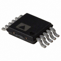
AD5446YRMZ Analog Devices Inc, AD5446YRMZ Datasheet - Page 20

AD5446YRMZ
Manufacturer Part Number
AD5446YRMZ
Description
IC DAC 14BIT MULTIPLYING 10-MSOP
Manufacturer
Analog Devices Inc
Datasheet
1.AD5446YRMZ.pdf
(28 pages)
Specifications of AD5446YRMZ
Data Interface
DSP, MICROWIRE™, QSPI™, Serial, SPI™
Design Resources
Versatile High Precision Programmable Current Sources Using DACs, Op Amps, and MOSFET Transistors (CN0151)
Number Of Bits
14
Number Of Converters
1
Voltage Supply Source
Single Supply
Power Dissipation (max)
50.5µW
Operating Temperature
-40°C ~ 125°C
Mounting Type
Surface Mount
Package / Case
10-MSOP, Micro10™, 10-uMAX, 10-uSOP
Resolution (bits)
14bit
Sampling Rate
2.7MSPS
Input Channel Type
Serial
Supply Voltage Range - Analog
2.5V To 5.5V
Supply Current
400nA
Digital Ic Case Style
SOP
Lead Free Status / RoHS Status
Lead free / RoHS Compliant
For Use With
EVAL-AD5446EBZ - BOARD EVALUATION FOR AD5446
Settling Time
-
Lead Free Status / RoHS Status
Lead free / RoHS Compliant, Lead free / RoHS Compliant
Available stocks
Company
Part Number
Manufacturer
Quantity
Price
Company:
Part Number:
AD5446YRMZ
Manufacturer:
ADI
Quantity:
352
Part Number:
AD5446YRMZ
Manufacturer:
ADI/亚德诺
Quantity:
20 000
AD5444/AD5446
SERIAL INTERFACE
The AD5444/AD5446 have an easy-to-use, 3-wire interface that
is compatible with SPI, QSPI, MICROWIRE, and DSP inter-
face standards. Data is written to the device in 16-bit words.
This 16-bit word consists of two control bits, 12 data bits or
14 data bits, as shown in Figure 44 and Figure 45. The AD5446
uses all 14 bits of DAC data while AD5444 uses 12 bits and
ignores the 2 LSBs.
Control Bit C1 and Control Bit C0 allow the user to load and
update the new DAC code and to change the active clock edge.
By default, the shift register clocks data on the falling edge, but
this can be changed via the control bits. If changed, the DAC
core is inoperative until the next data frame. A power cycle
resets this back to the default condition. On-chip, power-on
reset circuitry ensures the device powers on with zero scale
loaded to the DAC register and the I
Table 10. DAC Control Bits
C1
0
0
1
1
SYNC Function
SYNC is an edge-triggered input that acts as a frame synchroni-
zation signal. Data can be transferred into the device only while
SYNC is low. To start the serial data transfer, SYNC should be
taken low, observing the minimum SYNC falling to the SCLK
falling edge setup time, t
of the device, the interface powers up fully only when the device
is being written to, that is, on the falling edge of SYNC .
The SCLK and DIN input buffers are powered down on the
rising edge of SYNC .
C0
0
1
0
1
Function Implemented
Load and update (power-on default)
Disable SDO
No operation
Clock data to shift register on rising edge
4
. To minimize the power consumption
CONTROL BITS
CONTROL BITS
DB15 (MSB)
DB15 (MSB)
C1
C1
OUT
C0
C0
line.
DB11 DB10
DB13 DB12
Figure 44. AD5444 12-Bit Input Shift Register Contents
Figure 45. AD5446 14-Bit Input Shift Register Contents
DB11
DB9
DB10
DB8
DB7 DB6 DB5 DB4 DB3 DB2
DB9 DB8 DB7 DB6 DB5 DB4
Rev. C | Page 20 of 28
DATA BITS
DATA BITS
After the falling edge of the 16th SCLK pulse, bring SYNC high
to transfer data from the input shift register to the DAC register.
Daisy-Chain Mode
Daisy-chain mode is the default power-on mode. To disable
the daisy-chain function, write 01 to the control word. In daisy-
chain mode, the internal gating on the SCLK is disabled. The
SCLK is continuously applied to the input shift register when
SYNC is low. If more then 16 clock pulses are applied, the data
ripples out of the shift register and appears on the SDO line.
This data is clocked out on the rising edge of the SCLK (this
is the default; use the control word to change the active edge)
and is valid for the next device on the falling edge (default).
By connecting this line to the SDIN input on the next device in
the chain, a multidevice interface is constructed. Sixteen clock
pulses are required for each device in the system. Therefore, the
total number of clock cycles must equal 16 N , where N is the
number of devices in the chain.
When the serial transfer to all devices is complete, SYNC
should be taken high. This prevents any further data from
being clocked into the shift register. A burst clock containing
the exact number of clock cycles can be used, and SYNC can be
taken high some time later. After the rising edge of SYNC , data
is automatically transferred from each device’s input register to
the addressed DAC.
When the control bits = 10, the device is in no operation mode.
This can be useful in daisy-chain applications where the user
does not want to change the settings of a particular DAC in the
chain. Simply write 10 to the control bits for that DAC and the
following data bits are ignored.
DB1
DB3
DB0
DB2
DB1
DB0 (LSB)
DB0 (LSB)
X
DB0
X


