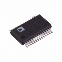
AD9761ARSZ Analog Devices Inc, AD9761ARSZ Datasheet - Page 10

AD9761ARSZ
Manufacturer Part Number
AD9761ARSZ
Description
IC DAC 10BIT DUAL 40MSPS 28-SSOP
Manufacturer
Analog Devices Inc
Datasheet
1.AD9761ARSZ.pdf
(24 pages)
Specifications of AD9761ARSZ
Data Interface
Parallel
Settling Time
35ns
Number Of Bits
10
Number Of Converters
2
Voltage Supply Source
Analog and Digital
Power Dissipation (max)
250mW
Operating Temperature
-40°C ~ 85°C
Mounting Type
Surface Mount
Package / Case
28-SSOP
Resolution (bits)
10bit
Sampling Rate
40MSPS
Input Channel Type
Parallel
Supply Voltage Range - Analogue
3V To 5.5V
Supply Voltage Range - Digital
2.7V To 5.5V
Supply
RoHS Compliant
Lead Free Status / RoHS Status
Lead free / RoHS Compliant
For Use With
AD9761-EBZ - BOARD EVAL FOR AD9761
Lead Free Status / RoHS Status
Lead free / RoHS Compliant
Available stocks
Company
Part Number
Manufacturer
Quantity
Price
Part Number:
AD9761ARSZ
Manufacturer:
ADI/亚德诺
Quantity:
20 000
FUNCTIONAL DESCRIPTION
Figure 4 shows a simplified block diagram of the AD9761. The
AD9761 is a complete dual-channel, high speed, 10-bit CMOS
DAC capable of operating up to a 40 MHz clock rate. It has
been optimized for the transmit section of wideband communica-
tion systems employing I and Q modulation schemes. Excellent
matching characteristics between channels reduce the need for
any external calibration circuitry. Dual matching 2 interpola-
tion filters included in the I and Q data path simplify any post
band-limiting filter requirements. The AD9761 interfaces with a
single 10-bit digital input bus that supports interleaved I and Q
input data.
Referring to Figure 4, the AD9761 consists of an analog sec-
tion and a digital section. The analog section includes matched
I and Q 10-bit DACs, a 1.20 V band gap voltage reference, and
a reference control amplifier.The digital section includes two 2
interpolation filters, segment decoding logic, and some additional
digital input interface circuitry. The analog and digital sections of
the AD9761 have separate power supply inputs (i.e., AVDD and
DVDD) that can operate independently. The digital supply can
operate over a 2.7 V to 5.5 V range, allowing it to accommodate
TTL as well as 3.3 V and 5 V CMOS logic families. The analog
supply must be restricted from 3.0 V to 5.5 V to maintain opti-
mum performance.
AD9761
SELECT INPUT
WRITE INPUT
DAC DATA
(10 BITS)
INPUTS
Figure 4. Dual DAC Functional Block Diagram
SLEEP
FREQUENCY DOMAIN
DCOM
TIME DOMAIN
CONTROL
MUX
LATCH
LATCH
Figure 5.Time and Frequency Domain Example of Digital Interpolation Filter
DVDD
Q
I
FUNDAMENTAL
CLOCK
2
f
CLOCK
2
2
INPUT DATA LATCH
GENERATOR
REFERENCE
AD9761
f
CLOCK
ACOM
f
1
BIAS
CLOCK
ST
2
2
IMAGE
DAC
DAC
Q
I
AVDD
f
CLOCK
REFLO
FSADJ
REFIO
COMP1
COMP2
COMP3
QOUTB
IOUTA
IOUTB
QOUTA
FUNDAMENTAL DIGITAL
SUPPRESSED
1
ST
OLD
IMAGE
1
f
CLOCK
–10–
2 INTERPOLATION FILTER
Each DAC consists of a large PMOS current source array capable
of providing up to 10 mA of full-scale current, I
divided into 15 equal currents that make up the four most signifi-
cant bits (MSBs). The next four bits or middle bits consist of 15
equal current sources whose values are 1/16 of an MSB current
source. The remaining LSBs are binary weighted fractions of
the middle bits’ current sources. All of these current sources are
switched to one of two output nodes (i.e., IOUTA or IOUTB)
via PMOS differential current switches.
The full-scale output current, I
from the same voltage reference and control amplifier, thus
ensuring excellent gain matching and drift characteristics
between DACs. I
external resistor, R
with both the reference control amplifier and voltage reference,
V
to the segmented current sources with the proper scaling factor.
I
The I and Q DACs are simultaneously updated on the rising
edge of CLOCK with digital data from their respective 2
digital interpolation filters. The 2 interpolation filters essen-
tially multiply the input data rate of each DAC by a factor of
2, relative to its original input data rate, while simultaneously
reducing the magnitude of the first image associated with the
DAC’s original input data rate. Since the AD9761 supports a
single 10-bit digital bus with interleaved I and Q input data, the
original I and Q input data rate before interpolation is one-half
the CLOCK rate. After interpolation, the data rate into each I
and Q DAC becomes equal to the CLOCK rate.
The benefits of an interpolation filter are illustrated in Figure 5,
which shows an example of the frequency and time domain rep-
resentation of a discrete time sine wave signal before and after
it is applied to a digital interpolation filter. Images of the sine
wave signal appear around multiples of the DAC’s input data
rate as predicted by the sampling theory. These undesirable
images will also appear at the output of a reconstruction DAC,
although modified by the DAC’s sin(x)/(x) response. In many
band-limited applications, these images must be suppressed by
an analog filter following the DAC. The complexity of this ana-
FILTER
OUTFS
f
f
CLOCK
REFIO
CLOCK
2
2
, sets the reference current, I
is exactly 16 times the value of I
f
CLOCK
NEW
1ST IMAGE
OUTFS
SET
. The external resistor in combination
can be set from 1 mA to 10 mA via an
OUTFS
f
DAC
CLOCK
DACs
2
REF
, of each DAC is regulated
, which is mirrored over
SIN(X)
REF
X
f
CLOCK
.
OUTFS
. Each array is
REV. C


