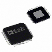
AD9777BSVZ Analog Devices Inc, AD9777BSVZ Datasheet - Page 39

AD9777BSVZ
Manufacturer Part Number
AD9777BSVZ
Description
IC DAC 16BIT DUAL 160MSPS 80TQFP
Manufacturer
Analog Devices Inc
Series
TxDAC+®r
Datasheet
1.AD9777BSVZ.pdf
(60 pages)
Specifications of AD9777BSVZ
Data Interface
Parallel
Settling Time
11ns
Number Of Bits
16
Number Of Converters
2
Voltage Supply Source
Analog and Digital
Power Dissipation (max)
410mW
Operating Temperature
-40°C ~ 85°C
Mounting Type
Surface Mount
Package / Case
80-TQFP Exposed Pad, 80-eTQFP, 80-HTQFP, 80-VQFP
Resolution (bits)
16bit
Sampling Rate
400MSPS
Input Channel Type
Parallel
Supply Voltage Range - Analog
3.1V To 3.5V
Supply Current
72.5mA
Lead Free Status / RoHS Status
Lead free / RoHS Compliant
For Use With
AD9777-EBZ - BOARD EVALUATION FOR AD9777
Lead Free Status / RoHS Status
Lead free / RoHS Compliant, Lead free / RoHS Compliant
Available stocks
Company
Part Number
Manufacturer
Quantity
Price
Company:
Part Number:
AD9777BSVZ
Manufacturer:
AD
Quantity:
1 000
Company:
Part Number:
AD9777BSVZ
Manufacturer:
ADI
Quantity:
182
Company:
Part Number:
AD9777BSVZ
Manufacturer:
Analog Devices Inc
Quantity:
10 000
Part Number:
AD9777BSVZ
Manufacturer:
ADI/亚德诺
Quantity:
20 000
Company:
Part Number:
AD9777BSVZRL
Manufacturer:
Analog Devices Inc
Quantity:
10 000
COMPLEX MODULATION AND IMAGE REJECTION
OF BASEBAND SIGNALS
In traditional transmit applications, a two-step upconversion is
done in which a baseband signal is modulated by one carrier to
an IF (intermediate frequency) and then modulated a second
time to the transmit frequency. Although this approach has
several benefits, a major drawback is that two images are created
near the transmit frequency. Only one image is needed, the other
being an exact duplicate. Unless the unwanted image is filtered,
typically with analog components, transmit power is wasted and
the usable bandwidth available in the system is reduced.
A more efficient method of suppressing the unwanted image
can be achieved by using a complex modulator followed by a
quadrature modulator. Figure 78 is a block diagram of a
quadrature modulator. Note that it is in fact the real output half
of a complex modulator. The complete upconversion can
actually be referred to as two complex upconversion stages, the
real output of which becomes the transmitted signal.
(IMAGINARY)
Figure 77. Implementation of a Complex Modulator
(REAL)
INPUT
INPUT
e
–jωt
= COSωt + jSINωt
90°
OUTPUT
(REAL)
OUTPUT
(IMAGINARY)
Rev. C | Page 39 of 60
The entire upconversion from baseband to transmit frequency
is represented graphically in Figure 79. The resulting spectrum
shown in Figure 79 represents the complex data consisting of
the baseband real and imaginary channels, now modulated onto
orthogonal (cosine and negative sine) carriers at the transmit
frequency. It is important to remember that in this application
(two baseband data channels), the image rejection is not
dependent on the data at either of the AD9777 input channels.
In fact, image rejection still occurs with either one or both of
the AD9777 input channels active. Note that by changing the
sign of the sinusoidal multiplying term in the complex
modulator, the upper sideband image could have been
suppressed while passing the lower one. This is easily done in
the AD9777 by selecting the e
purely complex terms, Figure 79 represents the two-stage
upconversion from complex baseband to carrier.
(IMAGINARY)
(REAL)
INPUT
INPUT
Figure 78. Quadrature Modulation
SINωt
90°
+jωt
bit (Register 01h, Bit 1). In
COSωt
OUTPUT
AD9777


