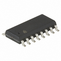
HI3338KIBZ Intersil, HI3338KIBZ Datasheet - Page 8

HI3338KIBZ
Manufacturer Part Number
HI3338KIBZ
Description
IC DAC 8BIT CMOS 16-SOIC
Manufacturer
Intersil
Datasheet
1.HI3338KIBZ.pdf
(9 pages)
Specifications of HI3338KIBZ
Settling Time
20ns
Number Of Bits
8
Data Interface
Parallel
Number Of Converters
1
Voltage Supply Source
Single Supply
Power Dissipation (max)
100mW
Operating Temperature
-40°C ~ 85°C
Mounting Type
Surface Mount
Package / Case
16-SOIC (0.300", 7.5mm Width)
Lead Free Status / RoHS Status
Lead free / RoHS Compliant
Applications
The output of the HI3338 can be resistively divided to match
a doubly terminated 50Ω or 75Ω line, although peak-to-peak
swings of less than 1V may result. The output magnitude will
also vary with the converter's output impedance. Figure 5
shows such an application. Note that because of the HCT
input structure, the HI3338 could be operated up to +7.5V
V
input voltages.
If larger voltage swings or better accuracy is desired, a high
speed output buffer, such as the HA-5033, HA-2542, or
CA3450, can be employed. Figure 6 shows a typical
application, with the output capable of driving ±2V into
multiple 50Ω terminated lines.
Operating and Handling Considerations
HANDLING
All inputs and outputs of CMOS devices have a network for
electrostatic protection during handling. Recommended
handling practices for CMOS devices are described in
AN6525. “Guide to Better Handling and Operation of CMOS
Integrated Circuits.”
DD
NOTES:
CLOCK
8 DATA
1. Both V
2. Keep nodal capacitance at CA3450 pin 3 as low as possible.
3. V
and V
BITS
+5V
1
/
OUT
4
inch.
REF
+
Range = ±3V at CA3450.
REF
+ supplies and still accept 0V to 5V CMOS
4.7µF
TAN
+ pin and 392Ω resistor should be bypassed within
0.1µF
CER.
1-7, 9
15
16
14
8
FIGURE 6. HI3338 AND CA3450 FOR DRIVING MULTIPLE COAXIAL LINES
8
D0 - D7
V
COMP
V
LE
DD
SS
HI3338
V
V
V
REF
REF
OUT
V
EE
+
-
12
13
11
10
4.7µF
TAN
+
+3.00V AT 25mA
0.1µF
CER.
1kΩ
HI3338
392Ω
10kΩ
ADJUST
OFFSET
1%
OPERATING
OPERATING VOLTAGE
During operation near the maximum supply voltage limit,
care should be taken to avoid or suppress power supply
turn-on and turn-off transients, power supply ripple, or
ground noise; any of these conditions must not cause the
absolute maximum ratings to be exceeded.
INPUT SIGNALS
To prevent damage to the input protection circuit, input
signals should never be greater than V
Input currents must not exceed 20mA even when the power
supply is off.
UNUSED INPUTS
A connection must be provided at every input terminal. All
unused input terminals must be connected to either V
GND, whichever is appropriate.
392Ω
14
1%
3
7, 8
+6V
-6V
+
CA3450
-
4, 5, 12, 13
4.7µF TAN
9
4.7µF
TAN
11
+
0.1µF CER.
5pF
+
6
0.1µF
CER.
R
R
V
OUT
UP TO 5 OUTPUT LINES
FOR R = 75Ω, 3 LINES
FOR R = 50Ω
= ± 1.5V
DD
PEAK
nor less than V
R
R
V
V
OUT
OUT
CC
N
1
SS
or
.


