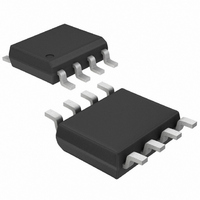
MAX5556ESA+ Maxim Integrated Products, MAX5556ESA+ Datasheet - Page 10

MAX5556ESA+
Manufacturer Part Number
MAX5556ESA+
Description
IC DAC STEREO AUDIO 8-SOIC
Manufacturer
Maxim Integrated Products
Specifications of MAX5556ESA+
Number Of Bits
16
Data Interface
Serial
Number Of Converters
2
Voltage Supply Source
Single Supply
Operating Temperature
-40°C ~ 85°C
Mounting Type
Surface Mount
Package / Case
8-SOIC (3.9mm Width)
Number Of Dac Outputs
2
Resolution
16 bit
Interface Type
Serial (3-Wire)
Supply Voltage (max)
5.5 V
Supply Voltage (min)
4.75 V
Maximum Operating Temperature
+ 85 C
Mounting Style
SMD/SMT
Maximum Power Dissipation
471 mW
Minimum Operating Temperature
- 40 C
Supply Current
13 mA
Lead Free Status / RoHS Status
Lead free / RoHS Compliant
Power Dissipation (max)
-
Settling Time
-
Lead Free Status / Rohs Status
Lead free / RoHS Compliant
Low-Cost Stereo Audio DACs
Figure 6. MAX5558 Data Format Timing
Figure 7. MAX5559 Data Format Timing
SCLK strobes the individual data bits at SDATA into the
DAC. The MAX5556–MAX5559 operate in one of two
modes: internal serial clock mode or external serial
clock mode.
The MAX5556–MAX5559 operate in external serial clock
mode when SCLK activity is detected. All four devices
return to internal serial clock mode if no SCLK signal is
detected for one LRCLK period. Figure 8 details the
external serial clock mode timing parameters.
10
LRCLK
SDATA
SCLK
LRCLK
SDATA
SCLK
_______________________________________________________________________________________
MSB
17
MSB
15
16
14
15
13
14
• RIGHT-JUSTIFIED, 16-BIT DATA
• INTERNAL SCLK = 32 x f
• INTERNAL SCLK = 48 x f
• RIGHT-JUSTIFIED, 18-BIT DATA
• INTERNAL SCLK = 64 x f
• INTERNAL SCLK = 48 x f
12
13
DATA DIRECTED TO OUTL
DATA DIRECTED TO OUTL
11
12
INTERNAL SERIAL CLOCK MODE
10
11
INTERNAL SERIAL CLOCK MODE
External SCLK Mode
10
Serial Clock (SCLK)
9
S
S
9
8
IF MCLK / LRCLK = 256 OR 512
IF MCLK / LRCLK = 384
S
S
IF MCLK / LRCLK = 256 OR 512
IF MCLK / LRCLK = 384
8
7
7
6
6
5
5
4
4
3
3
2
2
• RIGHT-JUSTIFIED, 16-BIT DATA
• DATA VALID ON RISING EDGE OF SCLK
• SCLK MUST HAVE AT LEAST 32 CYCLES PER LRCLK PERIOD
1
• RIGHT-JUSTIFIED, 18-BIT DATA
• DATA VALID ON RISING EDGE OF SCLK
• SCLK MUST HAVE AT LEAST 36 CYCLES PER LRCLK PERIOD
1
LSB
LSB
0
0
The MAX5556–MAX5559 transition from external serial
clock mode to internal serial clock mode if no SCLK
signal is detected for one LRCLK period. In internal
clock mode, SCLK is derived from and is synchronous
with MCLK and LRCLK (operation in internal clock
mode is identical to an external clock mode when
LRCLK is synchronized with MCLK). Figure 9 details
the internal serial clock mode timing parameters. Figure
10 details the generation of the internal clock.
EXTERNAL SERIAL CLOCK MODE
EXTERNAL SERIAL CLOCK MODE
MSB
MSB
15
17
16
14
15
13
14
12
13
11
12
10
DATA DIRECTED TO OUTR
11
DATA DIRECTED TO OUTR
9
10
8
9
7
8
6
7
5
6
Internal SCLK Mode
4
5
3
4
2
3
2
1
LSB
1
0
LSB
0


