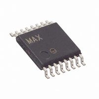
MAX5308EUE+ Maxim Integrated Products, MAX5308EUE+ Datasheet

MAX5308EUE+
Specifications of MAX5308EUE+
Related parts for MAX5308EUE+
MAX5308EUE+ Summary of contents
Page 1
... Control of Optical Components SPI and QSPI are trademarks of Motorola, Inc. MICROWIRE is a trademark of National Semiconductor, Corp. ________________________________________________________________ Maxim Integrated Products For pricing, delivery, and ordering information, please contact Maxim/Dallas Direct! at 1-888-629-4642, or visit Maxim’s website at www.maxim-ic.com. o Eight Highly Integrated 10-Bit DACs in 16-Pin TSSOP (6.4mm o Ultra-Low Glitch Energy < ...
Page 2
Low-Power, Low-Glitch, Octal 10-Bit Voltage- Output DACs with Serial Interface ABSOLUTE MAXIMUM RATINGS V to GND ............................................................. -0.3V to +6V DD All Other Pins to GND.................................-0. Continuous Power Dissipation (T = +70°C) A 16-Pin TSSOP (derate 9.4mW/°C above ...
Page 3
Low-Power, Low-Glitch, Octal 10-Bit Voltage- Output DACs with Serial Interface ELECTRICAL CHARACTERISTICS (continued +2.7V to +5.5V, GND = REF +5V +25°C PARAMETER DIGITAL INPUTS (SCLK, DIN, CS, LDAC, ...
Page 4
Low-Power, Low-Glitch, Octal 10-Bit Voltage- Output DACs with Serial Interface ELECTRICAL CHARACTERISTICS (continued +2.7V to +5.5V, GND = REF +5V +25°C PARAMETER TIMING CHARACTERISTICS Serial Clock ...
Page 5
Low-Power, Low-Glitch, Octal 10-Bit Voltage- Output DACs with Serial Interface (V = +5V +25°C, unless otherwise noted INTEGRAL NONLINEARITY vs. DIGITAL INPUT CODE 0.20 0.15 0.10 0.05 0 -0.05 -0.10 0 200 400 600 800 1000 ...
Page 6
Low-Power, Low-Glitch, Octal 10-Bit Voltage- Output DACs with Serial Interface (V = +5V +25°C, unless otherwise noted FULL-SCALE ERROR vs. LOAD CURRENT 0 -0.25 -0.50 -0.75 -1.00 -1.25 -1. +4.096V REF NORMALIZED TO 0.1mA ...
Page 7
Low-Power, Low-Glitch, Octal 10-Bit Voltage- Output DACs with Serial Interface PIN NAME 1 SCLK Serial Clock Input. Serial data is loaded on the falling edge of SCLK. 2 DIN Serial Data Input Load DAC. LDAC is an asynchronous active-low input ...
Page 8
Low-Power, Low-Glitch, Octal 10-Bit Voltage- Output DACs with Serial Interface Table 1. Serial Interface Configuration 16-BIT SERIAL WORD CONTROL BITS MSB D09 D08 D07 D06 D05 D04 D03 D02 D01 D00 ...
Page 9
Low-Power, Low-Glitch, Octal 10-Bit Voltage- Output DACs with Serial Interface V DD MAX5308 MAX5309 CS SCLK SERIAL TO PARALLEL DIN SHIFT REGISTER (MAX5309) CLR (MAX5308) DOUT LDAC Figure 1. Functional Diagram 20ns before the next write sequence since a write ...
Page 10
Low-Power, Low-Glitch, Octal 10-Bit Voltage- Output DACs with Serial Interface Table 2. Serial Interface Power-Up and Shutdown Commands CONTROL BITS DAC DAC DAC DAC ...
Page 11
Low-Power, Low-Glitch, Octal 10-Bit Voltage- Output DACs with Serial Interface SCLK DIN MAX5308 DOUT* CS *THE DOUT-SI CONNECTION IS NOT REQUIRED FOR WRITING TO THE MAX5308, BUT MAY BE USED FOR TRANSMISSION VERIFICATION PURPOSES. Figure 2. Connections for MICROWIRE and ...
Page 12
Low-Power, Low-Glitch, Octal 10-Bit Voltage- Output DACs with Serial Interface SCLK DIN X D15 X D15* D14* DOUT t CSS t CSPWH CS CLR *PREVIOUS INPUT DATA LDAC V _ OUT Figure 4. ...
Page 13
Low-Power, Low-Glitch, Octal 10-Bit Voltage- Output DACs with Serial Interface Table 3. Unipolar Code Table DAC CONTENTS ANALOG OUTPUT MSB LSB 1000 0000 01 1000 0000 REF ...
Page 14
Low-Power, Low-Glitch, Octal 10-Bit Voltage- Output DACs with Serial Interface INPUT REGISTERS SCLK DIN SHIFT REGISTER (MAX5309) CLR (MAX5308) DOUT INPUT REGISTERS LDAC MAX5308 MAX5309 V REF R1 REF MAX5308 MAX5309 DAC OUT Figure ...
Page 15
... Maxim cannot assume responsibility for use of any circuitry other than circuitry entirely embodied in a Maxim product. No circuit patent licenses are implied. Maxim reserves the right to change the circuitry and specifications without notice at any time. Maxim Integrated Products, 120 San Gabriel Drive, Sunnyvale, CA 94086 408-737-7600 ____________________ 15 © 2001 Maxim Integrated Products Printed USA is a registered trademark of Maxim Integrated Products ...


