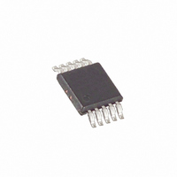
MAX5742EUB+ Maxim Integrated Products, MAX5742EUB+ Datasheet - Page 10

MAX5742EUB+
Manufacturer Part Number
MAX5742EUB+
Description
IC DAC 12BIT QUAD LP SER 10-UMAX
Manufacturer
Maxim Integrated Products
Datasheet
1.MAX5742EUB.pdf
(15 pages)
Specifications of MAX5742EUB+
Settling Time
4µs
Number Of Bits
12
Data Interface
Serial
Number Of Converters
4
Voltage Supply Source
Single Supply
Operating Temperature
-40°C ~ 85°C
Mounting Type
Surface Mount
Package / Case
10-MSOP, Micro10™, 10-uMAX, 10-uSOP
Number Of Dac Outputs
4
Resolution
12 bit
Interface Type
Serial (SPI)
Supply Voltage (max)
5.5 V
Supply Voltage (min)
2.7 V
Maximum Operating Temperature
+ 125 C
Mounting Style
SMD/SMT
Minimum Operating Temperature
- 40 C
Supply Current
420 uA
Voltage Reference
External
Lead Free Status / RoHS Status
Lead free / RoHS Compliant
Power Dissipation (max)
-
Lead Free Status / Rohs Status
Lead free / RoHS Compliant
12-Bit, Low-Power, Quad, Voltage-Output
DAC with Serial Interface
Table 1. Power-Down Mode Control
write sequence is initiated on a falling edge of CS. Not
keeping CS low during the first 15 SCLK cycles dis-
cards input data. The serial clock (SCLK) can idle
either high or low between transitions.
The MAX5742 has two internal registers per DAC, the
input register and the DAC register. The input register
holds the data that is waiting to be shifted to the DAC
register. All input registers can be loaded without
updating the output. This function is useful when all out-
puts need to be updated at the same time. The input
register can be made transparent. When the input reg-
ister is transparent, the data written into DIN loads
directly to the DAC register and the output is updated.
The DAC output is not updated until data is written to
the DAC register. See Table 2 for a list of serial-inter-
face programming commands.
10
X = Don’t care
C3
1
1
1
1
1
1
1
1
1
1
1
1
1
1
1
1
1
1
1
1
______________________________________________________________________________________
EXTENDED
CONTROL
C2
1
1
1
1
1
1
1
1
1
1
1
1
1
1
1
1
1
1
1
1
C1
1
1
1
1
1
1
1
1
1
1
1
1
1
1
1
1
1
1
1
1
C0
1
1
1
1
1
1
1
1
1
1
1
1
1
1
1
1
1
1
1
1
D11–D5
X
X
X
X
X
X
X
X
X
X
X
X
X
X
X
X
X
X
X
X
D4
0
0
0
0
0
0
0
0
0
0
0
0
0
0
0
0
1
1
1
1
DATA BITS
D3
0
0
0
0
0
0
0
0
1
1
1
1
1
1
1
1
0
0
0
0
D2
0
0
0
0
1
1
1
1
0
0
0
0
1
1
1
1
0
0
0
0
D1
0
0
1
1
0
0
1
1
0
0
1
1
0
0
1
1
0
0
1
1
D0
0
1
0
1
0
1
0
1
0
1
0
1
0
1
0
1
0
1
0
1
Power-On Reset (POR)
The MAX5742 has an internal POR circuit. At power-up all
DACs are powered-down and OUT_ is terminated to
GND through 100k resistors. Contents of input and DAC
registers are cleared to all zero. An 8µs recovery time
after issuing a wake-up command is needed before writ-
ing to the DAC registers. Power-down mode control com-
mands can be applied immediately with no recovery time.
C3-C0 are control bits. The data bits D11 to D0 are in
straight binary format. All zeros correspond to zero
scale and all ones correspond to full scale.
The digital inputs are compatible with CMOS logic. In
order to save power and reduce input to output coupling,
SCLK and DIN input buffers are powered down immedi-
ately after completion of shifting 16 bits into the input shift
register. A high to low transition at CS powers up SCLK
and DIN input buffers.
DESCRIPTION
DAC A-D
DAC A-D
DAC A-D
DAC A-D
DAC A
DAC A
DAC A
DAC A
DAC B
DAC B
DAC B
DAC B
DAC C
DAC C
DAC C
DAC C
DAC D
DAC D
DAC D
DAC D
DAC O/P, wakeup
Floating output
Output is terminated with 1k
Output is terminated with 100k
DAC O/P, wakeup
Floating output
Output is terminated with 1k
Output is terminated with 100k
DAC O/P, wakeup
Floating output
Output is terminated with 1k
Output is terminated with 100k
DAC O/P, wakeup
Floating output
Output is terminated with 1k
Output is terminated with 100k
DAC O/P, wakeup
Floating output
Output is terminated with 1k
Output is terminated with 100k
FUNCTION
Digital Inputs


