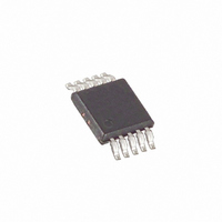
MAX5742EUB+ Maxim Integrated Products, MAX5742EUB+ Datasheet - Page 9

MAX5742EUB+
Manufacturer Part Number
MAX5742EUB+
Description
IC DAC 12BIT QUAD LP SER 10-UMAX
Manufacturer
Maxim Integrated Products
Datasheet
1.MAX5742EUB.pdf
(15 pages)
Specifications of MAX5742EUB+
Settling Time
4µs
Number Of Bits
12
Data Interface
Serial
Number Of Converters
4
Voltage Supply Source
Single Supply
Operating Temperature
-40°C ~ 85°C
Mounting Type
Surface Mount
Package / Case
10-MSOP, Micro10™, 10-uMAX, 10-uSOP
Number Of Dac Outputs
4
Resolution
12 bit
Interface Type
Serial (SPI)
Supply Voltage (max)
5.5 V
Supply Voltage (min)
2.7 V
Maximum Operating Temperature
+ 125 C
Mounting Style
SMD/SMT
Minimum Operating Temperature
- 40 C
Supply Current
420 uA
Voltage Reference
External
Lead Free Status / RoHS Status
Lead free / RoHS Compliant
Power Dissipation (max)
-
Lead Free Status / Rohs Status
Lead free / RoHS Compliant
The MAX5742 contains four 12-bit, voltage-output, low-
power digital-to-analog converters (DACs). Each DAC
employs a resistor string architecture that converts a
12-bit digital input word to an equivalent analog output
voltage proportional to the applied reference voltage.
The MAX5742 shares one reference input (REF)
between all four DACs. The MAX5742 includes rail-to-
rail output buffer amplifiers for each DAC, and input
logic for simple microprocessor (µP), and CMOS inter-
faces. The power-supply range is from +2.7V to +5.5V
(Functional Diagram). The MAX5742’s reference input
accepts a voltage range from 0 to V
mode the reference input is high impedance. The
MAX5742 is compatible with the 3-wire SPI, QSPI,
MICROWIRE and DSP serial interface with Schmitt-trig-
gered logic inputs.
The reference input accepts positive DC and AC sig-
nals. The voltage at REF sets the full-scale output volt-
age of the four DACs. The reference input voltage
range is 0 to V
voltage at REF can vary from GND to V
voltages (V
grammable voltage source as:
where D is the decimal equivalent of binary DAC input
code ranging from 0 to 4095. V
REF.
All DACs are internally buffered at the output. The
buffer amplifiers have both rail-to-rail common mode
Reference Input and DAC Output Range
7–10
PIN
1
2
3
4
5
6
OUT_
DD
V
OUTA –OUTD
) are represented by a digitally pro-
12-Bit, Low-Power, Quad, Voltage-Output
OUT_
. The impedance at REF is 45k . The
_______________________________________________________________________________________
NAME
SCLK
GND
V
REF
DIN
CS
DD
Detailed Description
= (V
Output Buffer Amplifiers
REF
✕
Chip-Select Input
Serial-Clock Input
Power-Supply Input
Ground
Serial Data Input
External Reference Voltage Input
DAC Voltage Outputs. Power-on reset sets DAC registers to zero, and internally connects
OUT to GND with 100k resistor.
D) / 2
REF
DD
12
is the voltage at
. In power-down
DD
. The output
DAC with Serial Interface
and (GND to V
are unity-gain stable with C
Buffer amplifiers are disabled during power-up and
individual DAC outputs are shorted to GND through a
100k
gether be powered-down by programming the input
register control bits. During power down, contents of
the input and DAC registers remain the same. On
wake-up, all DAC outputs are restored to their pre-
power-down voltage values.
In power-down mode, the DAC outputs are pro-
grammed to one of three output states, 1k , 100k , or
floating (Table 1). The REF input is high impedance
(2M
reference; therefore, the system reference does not
have to be powered-down. The DAC outputs return to
the values contained in the registers when brought out
of power-down. The recovery time, from total power-
down to power-up, is 8µs. This extra time is needed to
allow the internal bias to wake-up. Power-down mode
reduces current consumption to 0.3µA.
The MAX5742 digital interface is a standard 3-wire con-
nection compatible with SPI/QSPI/MICROWIRE/DSP
interfaces. The chip-select input (CS) frames the serial
data loading at DIN. Immediately following CS high-to-
low transition, the data is shifted synchronously and
latched into the input register on the falling edge of the
serial clock input (SCLK). After 16 bits have been
loaded into the serial input register, it transfers its con-
tents to the DAC latch. CS may then either be held low
or brought high. CS must be brought high for a mini-
mum of 80ns before the next write sequence, since a
typ) to conserve current drain from the system
resistor. Buffer amplifiers can individually or alto-
FUNCTION
REF
) output voltage range. The buffers
3-Wire Serial Interface
L
= 200pF and R
Pin Description
Power-Down Mode
L
= 5k .
9


