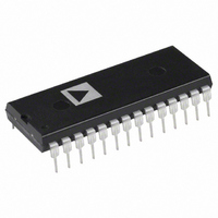
AD667JNZ Analog Devices Inc, AD667JNZ Datasheet - Page 4

AD667JNZ
Manufacturer Part Number
AD667JNZ
Description
IC DAC 12BIT W/BUFF LATCH 28-DIP
Manufacturer
Analog Devices Inc
Specifications of AD667JNZ
Settling Time
3µs
Number Of Bits
12
Number Of Converters
1
Voltage Supply Source
Dual ±
Power Dissipation (max)
1W
Operating Temperature
0°C ~ 70°C
Mounting Type
Through Hole
Package / Case
28-DIP (0.600", 15.24mm)
Resolution (bits)
12bit
Sampling Rate
500kSPS
Input Channel Type
Parallel
Supply Current
20mA
Digital Ic Case Style
DIP
No. Of Pins
28
Data Interface
Parallel
Lead Free Status / RoHS Status
Lead free / RoHS Compliant
Lead Free Status / RoHS Status
Lead free / RoHS Compliant, Lead free / RoHS Compliant
Available stocks
Company
Part Number
Manufacturer
Quantity
Price
Company:
Part Number:
AD667JNZ
Manufacturer:
PSPR
Quantity:
6 220
Part Number:
AD667JNZ
Manufacturer:
ADI/亚德诺
Quantity:
20 000
AD667
Model
AD667JN
AD667JP
AD667KN
AD667KP
AD667AD
AD667BD
AD667SD
AD667SE
AD667/883B –55 to +125
NOTES
*Refer to AD667/883B military data sheet.
1
2
THE AD667 OFFERS TRUE 12-BIT PERFORMANCE
OVER THE FULL TEMPERATURE RANGE
LINEARITY ERROR: Analog Devices defines linearity error as
the maximum deviation of the actual, adjusted DAC output
Output
Range
0 V to +10 V
0 V to +5 V
For details on grade and package offerings screened in accordance with MIL-STD-
D = Ceramic DIP; E = Leadless Ceramic Chip Carrier; N = Plastic DIP;
883, refer to the Analog Devices Military Products Databook or current AD667/
883B data sheet.
P = Plastic Leaded Chip.
10 V
5 V
2.5 V
l
Temperature
Range— C
0 to +70
0 to +70
0 to +70
0 to +70
25 to +85
–25 to +85
–55 to +125
–55 to +125
Digital
Input Codes
Offset Binary
Offset Binary
Offset Binary
Straight Binary
Straight Binary
ORDERING GUIDE
PLCC, LCC
Linearity
Error Max TC Max
@ +25 C
*
1/2 LSB
1/2 LSB
1/4 LSB
1/4 LSB
1/2 LSB
1/4 LSB
1/2 LSB
1/2 LSB
Gain
ppm/ C Package Option
30
30
15
15
30
15
30
30
*
Connect
Pin 9 to
1
1 and 2
2
1 and 2
2
Table I. Output Voltage Range Connections
Plastic DIP (N-28)
PLCC (P-28A)
Plastic DIP (N-28)
PLCC (P-28A)
Ceramic DIP (D-28)
Ceramic DIP (D-28)
Ceramic DIP (D-28)
LCC (E-28A)
*
Connect
Pin 1 to
9
2 and 9
3
2 and 9
3
PIN CONNECTIONS
2
–4–
Connect
Pin 2 to
NC
1 and 9
9
1 and 9
9
from the ideal analog output (a straight line drawn from 0 to FS
– 1 LSB) for any bit combination. The AD667 is laser trimmed
to 1/4 LSB (0.006% of FS) maximum error at +25 C for the K
and B versions and 1/2 LSB for the J, A and S versions.
MONOTONICITY: A DAC is said to be monotonic if the
output either increases or remains constant for increasing digital
inputs such that the output will always be a nondecreasing func-
tion of input. All versions of the AD667 are monotonic over
their full operating temperature range.
DIFFERENTIAL NONLINEARITY: Monotonic behavior re-
quires that the differential linearity error be less than 1 LSB
both at +25 C and over the temperature range of interest. Dif-
ferential nonlinearity is the measure of the variation in analog
value, normalized to full scale, associated with a 1 LSB change
in digital input code. For example, for a 10 volt full-scale out-
put, a change of 1 LSB in digital input code should result in a
2.44 mV change in the analog output (1 LSB = 10 V 1/4096 =
2.44 mV). If in actual use, however, a 1 LSB change in the
input code results in a change of only 0.61 mV (1/4 LSB) in
analog output, the differential linearity error would be –1.83 mV,
or –3/4 LSB. The AD667K and B grades have a max differential
linearity error of 1/2 LSB, which specifies that every step will be
at least 1/2 LSB and at most 1 1/2 LSB.
Connect
Pin 4 to
6 (Through 50
6 (Through 50
6 (Through 50
5 (or Optional Trim—See Figure 2)
5 (or Optional Trim—See Figure 2)
DIP
Fixed or 100
Fixed or 100
Fixed or 100
Trim Resistor)
Trim Resistor)
Trim Resistor)
REV. A


