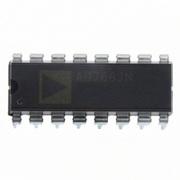
AD766JNZ Analog Devices Inc, AD766JNZ Datasheet - Page 4

AD766JNZ
Manufacturer Part Number
AD766JNZ
Description
IC DAC 16BIT W/VREF 16-DIP
Manufacturer
Analog Devices Inc
Series
DACPORT®r
Datasheet
1.AD766JNZ.pdf
(8 pages)
Specifications of AD766JNZ
Data Interface
Serial
Settling Time
1.5µs
Number Of Bits
16
Number Of Converters
1
Voltage Supply Source
Analog and Digital, Dual ±
Power Dissipation (max)
300mW
Operating Temperature
-40°C ~ 85°C
Mounting Type
Through Hole
Package / Case
16-DIP (0.300", 7.62mm)
Resolution (bits)
16bit
Sampling Rate
390kSPS
Input Channel Type
Serial
Supply Current
-14mA
Digital Ic Case Style
DIP
No. Of Pins
16
Lead Free Status / RoHS Status
Lead free / RoHS Compliant
Available stocks
Company
Part Number
Manufacturer
Quantity
Price
Part Number:
AD766JNZ
Manufacturer:
ADI/亚德诺
Quantity:
20 000
TOTAL HARMONIC DISTORTION
Total Harmonic Distortion (THD) is defined as the ratio of the
square root of the sum of the squares of the values of the har-
monics to the value of the fundamental input frequency. It is ex-
pressed in percent (%) or decibels (dB).
THD is a measure of the magnitude and distribution of integral
linearity error and differential linearity error. The distribution of
these errors may be different, depending on the amplitude of the
output signal. Therefore, to be most useful, THD should be
specified for both large and small signal amplitudes.
SETTLING TIME
Settling Time is the time required for the output to reach and
remain within a specified error band about its final value, mea-
sured from the digital input transition. It is the primary measure
of dynamic performance.
BIPOLAR ZERO ERROR
Bipolar Zero Error or midscale error is the deviation of the ac-
tual analog output from the ideal output (0 V) when the 2s
complement input code representing half scale (all 0s) is loaded
in the input register.
DIFFERENTIAL LINEARITY ERROR
Differential Linearity Error is the measure of the variation in
analog value, normalized to full scale, associated with a 1 LSB
change in the digital input. Monotonic behavior requires that
the differential linearity error not exceed 1 LSB in the negative
direction.
MONOTONICITY
A D/A converter is monotonic if the output either increases or
remains constant as the digital input increases.
SIGNAL-TO-NOISE RATIO
SNR is defined as the ratio of the fundamental to the square
root of the sum of the squares for the values of all the nonfun-
damental, nonharmonic signals for a specified bandwidth. SNR
is tested at full-scale input. The AD766 specifies SNR for
20 kHz and 250 kHz bandwidths.
AD766–Definition of Specifications
Figure 2. AD766 Serial Input Timing
–4–
FUNCTIONAL DESCRIPTION
Serial input data is clocked into the AD766’s shift register by
the falling edge of CLK. Data is presumed to be in twos
complement format with MSB (i.e., the sign bit) clocked in first.
The shift register converts the most recently clocked-in 16 bits
to a parallel word. The falling edge of the latch enable (LE) sig-
nal causes the most recent parallel word to be transferred to the
internal DAC input latch. See Figure 2 for detailed serial port
timing requirements.
The contents of the DAC input latch cause the 16-bit DAC to
generate a corresponding current. This 1 mA current is avail-
able directly on the I
To use the internal op amp, connect I
the summing junction pin, SJ (Pin 11) and connect the feedback
resistor pin, R
op amp is in the inverting configuration. Using the internal
3 k feedback resistor, this op amp will produce 3 V outputs.
One advantage of external pins at each end of the feedback
resistor is that it allows the user to implement a single pole
active low-pass filter simply by adding a capacitor across these
pins (Pins 10 and 13). The circuit can best be understood
redrawn as shown in Figure 1.
The frequency response from this filter will be
where R
Figure 1. Low-Pass Filter Using External Capacitor
F
is 3 k ( 20%).
F
(Pin 10) to V
V
OUT
OUT
I
OUT
pin.
(s)
OUT
R
(Pin 9). Note that the internal
F
C s 1
R
OUT
F
(Pin 13) directly to
REV. A


