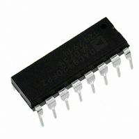
DAC8420FPZ Analog Devices Inc, DAC8420FPZ Datasheet - Page 20

DAC8420FPZ
Manufacturer Part Number
DAC8420FPZ
Description
IC DAC 12BIT QUAD SRL LP 16DIP
Manufacturer
Analog Devices Inc
Datasheet
1.DAC8420FPZ.pdf
(24 pages)
Specifications of DAC8420FPZ
Data Interface
Serial
Settling Time
8µs
Number Of Bits
12
Number Of Converters
4
Voltage Supply Source
Dual ±
Power Dissipation (max)
255mW
Operating Temperature
-40°C ~ 85°C
Mounting Type
Through Hole
Package / Case
16-DIP (0.300", 7.62mm)
Resolution (bits)
12bit
Sampling Rate
125kSPS
Input Channel Type
Serial
Supply Current
6mA
Digital Ic Case Style
DIP
No. Of Pins
16
Number Of Channels
4
Resolution
12b
Conversion Rate
125KSPS
Interface Type
Serial (3-Wire)
Single Supply Voltage (typ)
5V
Dual Supply Voltage (typ)
±5/±15V
Power Supply Requirement
Single/Dual
Output Type
Voltage
Integral Nonlinearity Error
±4LSB
Single Supply Voltage (min)
4.75V
Single Supply Voltage (max)
5.25V
Dual Supply Voltage (min)
±4.75V
Dual Supply Voltage (max)
±15.75V
Operating Temp Range
-40C to 85C
Operating Temperature Classification
Industrial
Mounting
Through Hole
Pin Count
16
Package Type
PDIP
Lead Free Status / RoHS Status
Lead free / RoHS Compliant
Lead Free Status / RoHS Status
Lead free / RoHS Compliant, Lead free / RoHS Compliant
DAC8420
DUAL WINDOW COMPARATOR
Often a comparator is needed to signal an out-of-range
warning. Combining the DAC8420 with a quad comparator
such as the
with adjustable trip points as shown in Figure 36. This circuit
can be operated with either a dual supply or a single supply. For
the A input channel, DAC B sets the low trip point, and DAC A
sets the upper trip point. The CMP04 has open-collector outputs
that are connected together in a wire-OR’ e d configuration to
generate an out-of-range signal. For example, when VINA
goes below the trip point set by DAC B, Comparator C2 pulls
the output down, turning on the red LED. The output can also
be used as a logic signal for further processing.
MC68HC11 MICROCONTROLLER INTERFACING
Figure 37 shows a serial interface between the DAC8420 and
the MC68HC11 8-bit microcontroller. The SCK output of the
port outputs the serial data to load into the SDI input of the
DAC. The port lines (PD5, PC0, PC1, and PC2) provide the
controls to the DAC as shown.
CMP04
0.1µF
5V SUPPLY
provides a simple dual window comparator
10
DIGITAL INPUTS
11
DAC8420
2
4
CONTROLS
V
GND
12
DIGITAL
IN
REF43
14
V
15
OUT 6
16
9
2.5V
GND
DAC A
DAC B
DAC C
DAC D
5
Figure 36. Dual Programmable Window Comparator
VREFHI
4
VREFLO
5V SUPPLY
1
8
VSS
Rev. B | Page 20 of 24
7
6
3
2
0.1µF
VOUTA
VOUTB
VOUTC
VOUTD
For correct operation, the MC68HC11 should be configured
such that its CPOL bit and CPHA bit are both set to 1. In this
configuration, serial data on MOSI of the MC68HC11 is valid
on the rising edge of the clock, which is the required timing for
the DAC8420. Data is transmitted in 8-bit bytes (MSB first),
with only eight rising clock edges occurring in the transmit
cycle. To load data to the input register of the DAC8420, PC0
is taken low and held low during the entire loading cycle. The
first eight bits are shifted in address first, immediately followed
by another eight bits in the second least-significant byte to load
the complete 16-bit word. At the end of the second byte load,
PC0 is then taken high. To prevent an additional advancing of
the internal shift register, SCK must already be asserted before
PC0 is taken high. To transfer the contents of the input shift
register to the DAC register, PD5 is then taken low, asserting the
LD input of the DAC and completing the loading process. PD5
should return high before the next load cycle begins. The CLR
input of the DAC8420 (controlled by the output PC1) provides
an asynchronous clear function.
VINA
VINB
11
10
5
4
7
6
9
8
CMP04
C1
C2
C3
C4
5V
12
3
MC68HC11*
Figure 37. MC68HC11 Microcontroller Interface
*ADDITIONAL PINS OMITTED FOR CLARITY.
0.1µF
(PD5) SS
14
13
2
1
MOSI
SCK
PC2
PC1
PC0
5V
604Ω
RED LED
5V
604Ω
RED LED
CLSEL
CLR
CS
LD
CLK
SDI
DAC8420*
OUT A
OUT B


