DAC8420FPZ Analog Devices Inc, DAC8420FPZ Datasheet - Page 8
DAC8420FPZ
Manufacturer Part Number
DAC8420FPZ
Description
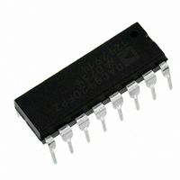
IC DAC 12BIT QUAD SRL LP 16DIP
Manufacturer
Analog Devices Inc
Datasheet
1.DAC8420FPZ.pdf
(24 pages)
Specifications of DAC8420FPZ
Data Interface
Serial
Settling Time
8µs
Number Of Bits
12
Number Of Converters
4
Voltage Supply Source
Dual ±
Power Dissipation (max)
255mW
Operating Temperature
-40°C ~ 85°C
Mounting Type
Through Hole
Package / Case
16-DIP (0.300", 7.62mm)
Resolution (bits)
12bit
Sampling Rate
125kSPS
Input Channel Type
Serial
Supply Current
6mA
Digital Ic Case Style
DIP
No. Of Pins
16
Number Of Channels
4
Resolution
12b
Conversion Rate
125KSPS
Interface Type
Serial (3-Wire)
Single Supply Voltage (typ)
5V
Dual Supply Voltage (typ)
±5/±15V
Power Supply Requirement
Single/Dual
Output Type
Voltage
Integral Nonlinearity Error
±4LSB
Single Supply Voltage (min)
4.75V
Single Supply Voltage (max)
5.25V
Dual Supply Voltage (min)
±4.75V
Dual Supply Voltage (max)
±15.75V
Operating Temp Range
-40C to 85C
Operating Temperature Classification
Industrial
Mounting
Through Hole
Pin Count
16
Package Type
PDIP
Lead Free Status / RoHS Status
Lead free / RoHS Compliant
Lead Free Status / RoHS Status
Lead free / RoHS Compliant, Lead free / RoHS Compliant


DAC8420
PIN CONFIGURATIONS AND FUNCTION DESCRIPTIONS
Table 5. Pin Function Descriptions
Pin No.
1
4
5
7, 6, 3, 2
8
9
10
11
12
13
14
15
16
VREFLO
Mnemonic
VDD
VREFLO
VREFHI
VOUTA through VOUTD
VSS
GND
SDI
CLK
CS
NC
LD
CLR
CLSEL
VREFHI
VOUTD
VOUTC
VOUTB
VOUTA
VDD
VSS
Figure 4. PDIP and CERDIP
1
2
3
4
5
6
7
8
NC = NO CONNECT
(Not to Scale)
DAC8420
TOP VIEW
16
15
14
13
12
10
11
9
CLSEL
CLR
LD
NC
CS
CLK
SDI
GND
Description
Positive Power Supply, 5 V to 15 V.
Reference Input. Lower DAC ladder reference voltage input, equal to zero-scale output. Allowable
range is V
Reference Input. Upper DAC ladder reference voltage input. Allowable range is (V
(V
Buffered DAC Analog Voltage Outputs.
Negative Power Supply, 0 V to −15 V.
Power Supply, Digital Ground.
Serial Data Input. Data presented to this pin is loaded into the internal serial-parallel shift register,
which shifts data in, beginning with DAC Address Bit A1. This input is ignored when CS is high. SDI
is CMOS/TTL compatible. The format of the 16-bit serial word is shown in Table 8.
System Serial Data Clock Input, TTL/CMOS Levels. Data presented to the input SDI is shifted into
the internal serial-parallel input register on the rising edge of clock. This input is logically OR’ed
with CS.
Control Input, Device Chip Select, Active Low. This input is logically OR’ed with the clock and
disables the serial data register input when high. When low, data input clocking is enabled (see
Table 6). CS is CMOS/TTL compatible.
No Connect = Don’t Care.
Control Input, Asynchronous DAC Register Load Control, Active Low. The data currently contained
in the serial input shift register is shifted out to the DAC data registers on the falling edge of LD,
independent of CS. Input data must remain stable while LD is low. LD is CMOS/TTL compatible.
Control Input, Asynchronous Clear, Active Low. Sets internal data Register A through Register D to
zero or midscale, depending on current state of CLSEL. The data in the serial input shift register is
unaffected by this control. CLR is CMOS/TTL compatible.
Control Input, Determines action of CLR. If high, a clear command sets the internal DAC Register A
through Register D to midscale (0x800). If low, the registers are set to zero (0x000). CLSEL is CMOS/
TTL compatible.
VREFLO
+ 2.5 V).
SS
to (V
VREFHI
Rev. B | Page 8 of 24
− 2.5 V).
VREFLO
VREFHI
VOUTD
VOUTC
VOUTB
VOUTA
VDD
VSS
1
2
3
4
5
6
7
8
NC = NO CONNECT
Figure 5. SOIC
(Not to Scale)
DAC8420
TOP VIEW
16
15
14
13
12
10
11
9
CLSEL
CLR
LD
NC
CS
CLK
SDI
GND
DD
− 2.5 V) to
Related parts for DAC8420FPZ
Image
Part Number
Description
Manufacturer
Datasheet
Request
R

Part Number:
Description:
Analog Standard Cell 8-Bit Digital to Analog Converter
Manufacturer:
AMSCO [austriamicrosystems AG]
Datasheet:

Part Number:
Description:
±1.7g Dual-Axis IMEMS Accelerometer Evaluation Board
Manufacturer:
Analog Devices Inc
Datasheet:

Part Number:
Description:
Inertial Sensor Evaluation System
Manufacturer:
Analog Devices Inc
Datasheet:
Part Number:
Description:
Manufacturer:
Analog Devices Inc
Datasheet:
Part Number:
Description:
Manufacturer:
Analog Devices Inc
Datasheet:
Part Number:
Description:
Manufacturer:
Analog Devices Inc
Datasheet:
Part Number:
Description:
Manufacturer:
Analog Devices Inc
Datasheet:
Part Number:
Description:
Manufacturer:
Analog Devices Inc
Datasheet:
Part Number:
Description:
Manufacturer:
Analog Devices Inc
Datasheet:
Part Number:
Description:
Manufacturer:
Analog Devices Inc
Datasheet:
Part Number:
Description:
Manufacturer:
Analog Devices Inc
Datasheet:
Part Number:
Description:
Manufacturer:
Analog Devices Inc
Datasheet:
Part Number:
Description:
Manufacturer:
Analog Devices Inc
Datasheet: