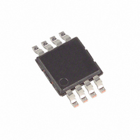
MAX548AEUA+ Maxim Integrated Products, MAX548AEUA+ Datasheet - Page 13

MAX548AEUA+
Manufacturer Part Number
MAX548AEUA+
Description
IC DAC 8BIT DUAL ASYNCH 8-UMAX
Manufacturer
Maxim Integrated Products
Datasheet
1.MAX550ACUA.pdf
(16 pages)
Specifications of MAX548AEUA+
Settling Time
4µs
Number Of Bits
8
Data Interface
Serial
Number Of Converters
1
Voltage Supply Source
Single Supply
Operating Temperature
-40°C ~ 85°C
Mounting Type
Surface Mount
Package / Case
8-MSOP, Micro8™, 8-uMAX, 8-uSOP,
Number Of Dac Outputs
2
Resolution
8 bit
Interface Type
Serial (SPI)
Supply Voltage (max)
5.5 V
Supply Voltage (min)
2.5 V
Maximum Operating Temperature
+ 85 C
Mounting Style
SMD/SMT
Minimum Operating Temperature
- 40 C
Supply Current
0.55 mA
Voltage Reference
External
Lead Free Status / RoHS Status
Lead free / RoHS Compliant
Power Dissipation (max)
-
Lead Free Status / Rohs Status
Lead free / RoHS Compliant
The MAX548A/MAX549A/MAX550A serial interface is
SPI/QSPI and Microwire compatible. For SPI/QSPI, clear
the CPOL and CPHA bits (CPOL = 0 and CPHA = 0).
CPOL = 0 sets the clock idle state to zero, and CPHA =
0 changes data at SCLK’s falling edge. This is the
Microwire default condition. If a serial port is not avail-
able on your microprocessor, three bits of a parallel port
can be used to emulate a serial port by bit manipulation.
Operate the serial clock only when necessary, to mini-
mize digital feedthrough at the DAC registers.
Connect GND to the highest quality ground available.
Bypass V
The reference input can be used without bypassing.
However, for optimum line/load-transient response and
noise performance, bypass the reference input with a
0.1µF to 4.7µF capacitor to GND.
Table 6. Analog Output vs. Code
Note: 1LSB = V
__________Applications Information
_____________________________________________Pin Configurations (continued)
D7
1
1
1
0
0
0
TOP VIEW
8-Bit Voltage-Output DACs in µMAX Package
DD
D6
1
0
0
1
0
0
with a 0.1µF to 0.22µF capacitor to GND.
REF
OUTA
GND
DIN
CS
x 2
______________________________________________________________________________________
1
2
4
3
+2.5V to +5.5V, Low-Power, Single/Dual,
and Ground Considerations
-8
D5
1
0
0
1
0
0
= V
DIP/ MAX
MAX549A
REF
Microprocessor Interfacing
DAC CONTENTS
(1 / 256); ANALOG OUTPUT = +V
D4
1
0
0
1
0
0
6
8
7
5
Power-Supply
D3
V
REF
OUTB
SCLK
1
0
0
1
0
0
DD
D2
1
0
0
1
0
0
D1
1
0
0
1
0
0
REF
Careful PC board layout minimizes crosstalk in DAC regis-
ters, the reference, and the digital inputs. Separate analog
traces by running ground traces between them. Make sure
that high-frequency digital lines are not routed parallel to
analog lines.
High-speed data at any of the digital input pins can
couple through a DAC’s internal stray package capaci-
tance and cause noise (digital feedthrough) at the DAC
output, even though LDAC and/or CS are held high
(see Typical Operating Characteristics ). Test digital
feedthrough by holding LDAC and/or CS high and tog-
gling the digital inputs from all 1s to all 0s.
Due to internal stray capacitance, higher frequency analog
input signals at REF can couple to the output, even when
the input digital code is all 0s. This condition is shown in
the MAX549A/MAX550A Reference AC Feedthrough vs.
Frequency graph in the Typical Operating Characteristics .
Test analog feedthrough by setting all DAC outputs to 0V
and sweeping REF.
(I / 256), where I = Integer Value of Digital Input.
D0
1
1
0
1
1
0
GND
OUT
DIN
CS
+V
1
2
4
3
REF
ANALOG OUTPUT (V)
+V
+V
+V
(128 / 256) = +V
DIP/ MAX
+V
MAX550A
REF
REF
REF
REF
(255 / 256)
(129 / 256)
(127 / 256)
AC Considerations
(1 / 256)
0
Analog Feedthrough
Digital Feedthrough
6
8
7
5
REF
V
REF
LDAC
SCLK
DD
/ 2
13


