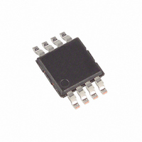
MAX548AEUA+ Maxim Integrated Products, MAX548AEUA+ Datasheet - Page 7

MAX548AEUA+
Manufacturer Part Number
MAX548AEUA+
Description
IC DAC 8BIT DUAL ASYNCH 8-UMAX
Manufacturer
Maxim Integrated Products
Datasheet
1.MAX550ACUA.pdf
(16 pages)
Specifications of MAX548AEUA+
Settling Time
4µs
Number Of Bits
8
Data Interface
Serial
Number Of Converters
1
Voltage Supply Source
Single Supply
Operating Temperature
-40°C ~ 85°C
Mounting Type
Surface Mount
Package / Case
8-MSOP, Micro8™, 8-uMAX, 8-uSOP,
Number Of Dac Outputs
2
Resolution
8 bit
Interface Type
Serial (SPI)
Supply Voltage (max)
5.5 V
Supply Voltage (min)
2.5 V
Maximum Operating Temperature
+ 85 C
Mounting Style
SMD/SMT
Minimum Operating Temperature
- 40 C
Supply Current
0.55 mA
Voltage Reference
External
Lead Free Status / RoHS Status
Lead free / RoHS Compliant
Power Dissipation (max)
-
Lead Free Status / Rohs Status
Lead free / RoHS Compliant
edge on CS programs the DAC. The input registers can
be loaded independently or simultaneously without
updating the DAC registers. This allows both DAC reg-
isters to be updated simultaneously with different digital
values. The DAC outputs reflect the data stored in the
DAC registers. LDAC can be used to asynchronously
update the DAC registers independently of CS
(MAX548A/MAX550A). With C1 set high, setting C0 in
the control word forces the DAC register(s) to be
updated on LDAC’s falling edge, rather than CS’s rising
edge (Table 1).
The MAX548A/MAX549A/MAX550A have an internal
power-on reset. At power-up, all internal registers are
reset to zero; therefore, an initialization write sequence
is not necessary.
Table 1. Control-Byte/Input-Word Bit Definitions
X = Don’t care
CONTROL BYTE
DATA
BYTE
8-Bit Voltage-Output DACs in µMAX Package
* Clocked in first
_______________________________________________________________________________________
+2.5V to +5.5V, Low-Power, Single/Dual,
BIT NAME
UB1*
UB2
UB3
D0**
C2
C2
C1
C1
C0
C0
D7
D6
D5
D4
D3
D2
D1
A1
A1
A0
A0
** Clocked in last
STATE
—
—
—
—
—
—
—
—
X
X
X
0
1
0
1
0
1
0
1
0
1
Initialization
Unassigned Bit 1
Unassigned Bit 2
Unassigned Bit 3
Power-Up Mode
Power-Down Mode
DAC Register Load Operation Disabled
DAC Register Load Operation Enabled
DAC Register Updated on CS’s Rising Edge
DAC Register Updated on LDAC’s Falling Edge (MAX549A = Don’t Care)
Do Not Address DAC B (MAX550A = Don’t Care)
Address DAC B (MAX550A = Don’t Care)
Do Not Address DAC A
Address DAC A
DAC Data Bit 7 (MSB)
DAC Data Bit 6
DAC Data Bit 5
DAC Data Bit 4
DAC Data Bit 3
DAC Data Bit 2
DAC Data Bit 1
DAC Data Bit 0 (LSB)
The control byte determines which input registers/DAC
registers are updated (Table 1). The DAC input regis-
ters are updated on the rising edge of CS. The DAC
registers can be updated on CS’s rising edge or on
LDAC’s falling edge after CS goes high. Bit C0 of the
control byte determines how the DAC registers are
updated for the MAX548A/MAX550A. The MAX549A
has no LDAC pin; the DAC registers are always up-
dated on CS’s rising edge (C0 in the control byte has
no effect).
Tables 2, 3, and 4 list the serial-input command format
for the MAX548A, MAX549A, and MAX550A, respec-
tively. The 16-bit input word consists of an 8-bit control
byte and an 8-bit data byte. The control byte is not
decoded internally. Every control bit performs one
Serial-Input Data Format and Control Codes
OPERATION
7


