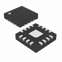
MAX5138BGTE+ Maxim Integrated Products, MAX5138BGTE+ Datasheet - Page 2

MAX5138BGTE+
Manufacturer Part Number
MAX5138BGTE+
Description
IC DAC 16BIT SGL 16-TQFN
Manufacturer
Maxim Integrated Products
Datasheet
1.MAX5139GTE.pdf
(17 pages)
Specifications of MAX5138BGTE+
Settling Time
5µs
Number Of Bits
16
Data Interface
DSP, I²C, MICROWIRE™, Parallel, QSPI™, SPI™
Number Of Converters
1
Voltage Supply Source
Analog and Digital
Operating Temperature
-40°C ~ 105°C
Mounting Type
Surface Mount
Package / Case
16-TQFN Exposed Pad
Interface Type
Serial (SPI, QSPI, Microwire, DSP)
Supply Voltage (max)
5.25 V
Supply Voltage (min)
2.7 V
Maximum Operating Temperature
+ 105 C
Mounting Style
SMD/SMT
Maximum Power Dissipation
1176.5 mW
Minimum Operating Temperature
- 40 C
Supply Current
1 mA
Lead Free Status / RoHS Status
Lead free / RoHS Compliant
Power Dissipation (max)
-
Lead Free Status / Rohs Status
Lead free / RoHS Compliant
Low-Power, Single, 16-/12-Bit,
Buffered Voltage-Output DACs
ABSOLUTE MAXIMUM RATINGS
AVDD to AGND ........................................................-0.3V to +6V
DVDD to AGND ........................................................-0.3V to +6V
OUT to AGND...............................................-0.3V to the lower of
REFI, REFO, M/Z to AGND ...........................-0.3V to the lower of
SCLK, DIN, CS to AGND ..............................-0.3V to the lower of
LDAC, READY to AGND...............................-0.3V to the lower of
ELECTRICAL CHARACTERISTICS
(V
T
Stresses beyond those listed under “Absolute Maximum Ratings” may cause permanent damage to the device. These are stress ratings only, and functional
operation of the device at these or any other conditions beyond those indicated in the operational sections of the specifications is not implied. Exposure to
absolute maximum rating conditions for extended periods may affect device reliability.
2
STATIC ACCURACY (Notes 1, 2)
Resolution
MAX5138 Integral Nonlinearity
MAX5139 Integral Nonlinearity
Differential Nonlinearity
Offset Error
Offset-Error Drift
Gain Error
Gain Temperature Coefficient
REFERENCE INPUT
Reference-Input Voltage Range
Reference Input Impedance
INTERNAL REFERENCE
Reference Voltage
Refer ence Tem p er atur e C oeffi ci ent
Reference Output Impedance
Line Regulation
Maximum Capacitive Load
A
AVDD
= T
_______________________________________________________________________________________
MIN
= 2.7V to 5.25V, V
to T
PARAMETER
MAX
, unless otherwise noted. Typical values are at T
DVDD
= 2.7V to 5.25V, V
SYMBOL
V
V
(DVDD + 0.3V) and +6V
(DVDD + 0.3V) and +6V
(AVDD + 0.3V) and +6V
(AVDD + 0.3V) and +6V
DNL
INL
INL
REFO
OE
GE
C
REFI
N
R
MAX5138
MAX5139
V
AVDD = 5.25V
V
Guaranteed monotonic
(Note 4)
(Note 4)
AVDD = 3V to 5.25V
AVDD = 2.7V to 3V
T
(Note 5)
AVDD
A =
REFI
REFI
+25°C
= 5V,
= 5V, AVDD = 5.25V
≥ V
DVDD
CONDITIONS
, V
A
AGND
= +25°C.)
Continuous Power Dissipation (T
Maximum Current into Any Input or Output
Maximum Current into M/Z Pin ...........................................±5mA
Operating Temperature Range .........................-40°C to +105°C
Storage Temperature Range .............................-65°C to +150°C
Lead Temperature (soldering, 10s) .................................+300°C
( N ote 3)
T
A
16-Pin TQFN (derate at 14.7mW/°C above +70°C) ..1176.5mW
with the Exception of M/Z Pin .......................................±50mA
= +25°C
= 0, V
REFI
= V
AVDD
- 0.25V, C
2.437
MIN
-1.0
-0.5
-10
16
12
-9
-1
2
2
A
= +70°C)
OUT
±0.25
2.440
±0.2
TYP
113
100
0.1
±2
±1
±4
±2
10
1
= 200pF, R
AVDD -
AVDD
2.443
MAX
+1.0
+0.5
+11
+10
0.2
±6
+1
25
OUT
% of FS
ppm/°C
UNITS
ppm/V
= 10kΩ,
µV/°C
FS/°C
ppm
LSB
LSB
LSB
Bits
mV
kΩ
nF
Ω
V
V


