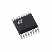
LTC2600IGN Linear Technology, LTC2600IGN Datasheet - Page 15

LTC2600IGN
Manufacturer Part Number
LTC2600IGN
Description
IC DAC R-R 16-BIT OCTAL 16-SSOP
Manufacturer
Linear Technology
Datasheet
1.LTC2620CUFDPBF.pdf
(20 pages)
Specifications of LTC2600IGN
Settling Time
10µs
Number Of Bits
16
Data Interface
Serial
Number Of Converters
8
Voltage Supply Source
Single Supply
Power Dissipation (max)
20mW
Operating Temperature
-40°C ~ 85°C
Mounting Type
Surface Mount
Package / Case
16-SSOP
Lead Free Status / RoHS Status
Contains lead / RoHS non-compliant
Available stocks
Company
Part Number
Manufacturer
Quantity
Price
Part Number:
LTC2600IGN
Manufacturer:
LT/凌特
Quantity:
20 000
Part Number:
LTC2600IGN#TRPBF
Manufacturer:
LINEAR/凌特
Quantity:
20 000
OPERATION
The GND pin functions both as the node to which the refer-
ence and output voltages are referred and as a return path
for power currents in the device. Because of this, careful
thought should be given to the grounding scheme and
board layout in order to ensure rated performance.
The PC board should have separate areas for the analog
and digital sections of the circuit. This keeps digital signals
away from sensitive analog signals and facilitates the use
of separate digital and analog ground planes which have
minimal capacitive and resistive interaction with each
other.
Digital and analog ground planes should be joined at only
one point, establishing a system star ground as close to
the device’s ground pin as possible. Ideally, the analog
ground plane should be located on the component side of
the board, and should be allowed to run under the part to
shield it from noise. Analog ground should be a continuous
and uninterrupted plane, except for necessary lead pads
and vias, with signal traces on another layer.
The GND pin of the part should be connected to analog
ground. Resistance from the GND pin to system star
ground should be as low as possible. Resistance here will
add directly to the effective DC output impedance of the
device (typically 0.025Ω), and will degrade DC crosstalk.
Note that the LTC2600/LTC2610/LTC2620 are no more
susceptible to these effects than other parts of their type;
on the contrary, they allow layout-based performance
improvements to shine rather than limiting attainable
performance with excessive internal resistance.
Rail-to-Rail Output Considerations
In any rail-to-rail voltage output device, the output is limited
to voltages within the supply range.
Since the analog outputs of the device cannot go below
ground, they may limit for the lowest codes as shown
in Figure 3b. Similarly, limiting can occur near full scale
when the REF pin is tied to V
full-scale error (FSE) is positive, the output for the highest
codes limits at V
limiting can occur if V
Offset and linearity are defi ned and tested over the region
of the DAC transfer function where no output limiting can
occur.
LTC2600/LTC2610/LTC2620
CC
as shown in Figure 3c. No full-scale
REF
is less than V
CC
. If V
REF
= V
CC
CC
– FSE.
and the DAC
15
2600fe


