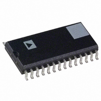
AD9760AR50 Analog Devices Inc, AD9760AR50 Datasheet - Page 13

AD9760AR50
Manufacturer Part Number
AD9760AR50
Description
IC DAC 10BIT 50MSPS 28-SOIC
Manufacturer
Analog Devices Inc
Series
TxDAC®r
Datasheet
1.AD9760ARUZ.pdf
(23 pages)
Specifications of AD9760AR50
Rohs Status
RoHS non-compliant
Settling Time
35ns
Number Of Bits
10
Number Of Converters
1
Voltage Supply Source
Analog and Digital
Power Dissipation (max)
175mW
Operating Temperature
-40°C ~ 85°C
Mounting Type
Surface Mount
Package / Case
28-SOIC (7.5mm Width)
Resolution (bits)
10bit
Input Channel Type
Parallel
Digital Ic Case Style
SOIC
No. Of Pins
28
Operating Temperature Range
-40°C To +85°C
Msl
MSL 3 - 168 Hours
Data Interface
Parallel
For Use With
AD9760-EBZ - BOARD EVAL FOR AD9760
Lead Free Status / RoHS Status
Contains lead / RoHS non-compliant
Available stocks
Company
Part Number
Manufacturer
Quantity
Price
Part Number:
AD9760AR50
Manufacturer:
ADI/亚德诺
Quantity:
20 000
The optimum distortion performance for any reconstructed
waveform is obtained with a 0.1 µF external capacitor installed.
Thus, if I
capacitor is recommended. Also, since the control amplifier is
optimized for low power operation, multiplying applications
requiring large signal swings should consider using an external
control amplifier to enhance the application’s overall large signal
multiplying bandwidth and/or distortion performance.
There are two methods in which I
R
which the internal reference is disabled, and the common-mode
voltage of REFIO is varied over its compliance range of 1.25 V
to 0.10 V. REFIO can be driven by a single-supply amplifier or
DAC, allowing I
input impedance of REFIO is approximately 1 MΩ, a simple,
low cost R-2R ladder DAC configured in the voltage mode
topology may be used to control the gain. This circuit is shown
in Figure 43 using the AD7524 and an external 1.2 V reference,
the AD1580.
The second method may be used in a dual-supply system in
which the common-mode voltage of REFIO is fixed and I
varied by an external voltage, V
fier. An example of this method is shown in Figure 44 where
the internal reference is used to set the common-mode voltage
of the control amplifier to 1.20 V. The external voltage, V
referenced to ACOM and should not exceed 1.2 V. The value
of R
and 625 µA, respectively. The associated equations in Figure 44
can be used to determine the value of R
REV. B
SET
SET
. The first method is suitable for a single-supply system in
V
1 F
is such that I
Figure 44. Dual-Supply Gain Control Circuit
GC
REF
is fixed for an application, a 0.1 µF ceramic chip
R
REF
SET
to be varied for a fixed R
REFMAX
I
WITH V
I
REF
REF
AD1580
= (1.2 – V
GC
FS ADJ
REFIO
1.2V
+1.2V REF
and I
AD9760
< V
AVDD
GC
GC
REFIO
REFLO
)/R
BANDLIMITING
REF
, applied to R
REFMIN
SET
CAPACITOR
AND 62.5 A
OPTIONAL
can be varied for a fixed
SET
OUT2
OUT1
50pF
do not exceed 62.5 µA
Figure 43. Single-Supply Gain Control Circuit
.
AGND
R
COMP1
SET
AD7524
FB
I
REF
CURRENT
SET
SOURCE
. Since the
ARRAY
AVDD
DB7–DB0
via an ampli-
AVDD
625A
V
DD
V
REF
REF
GC
R
, is
SET
is
0.1V TO 1.2V
–13–
I
V
REF
REF
In some applications, the user may elect to use an external con-
trol amplifier to enhance the multiplying bandwidth, distortion
performance and/or settling time. External amplifiers capable of
driving a 50 pF load such as the AD817 are suitable for this
purpose. It is configured in such a way that it is in parallel with
the weaker internal reference amplifier as shown in Figure 45.
In this case, the external amplifier simply overdrives the weaker
reference control amplifier. Also, since the internal control
amplifier has a limited current output, it will sustain no damage
if overdriven.
ANALOG OUTPUTS
The AD9760 produces two complementary current outputs,
I
differential operation. I
complementary single-ended voltage outputs, V
via a load resistor, R
Function section by Equations 5 through 8. The differential
voltage, V
converted to a single-ended voltage via a transformer or differ-
ential amplifier configuration. The ac performance of the AD9760
is optimum and specified using a differential transformer
coupled output in which the voltage swing at I
limited to ± 0.5 V. If a single-ended unipolar output is desirable,
I
The distortion and noise performance of the AD9760 can be
enhanced when the AD9760 is configured for differential opera-
tion. The common-mode error sources of both I
can be significantly reduced by the common-mode rejection of a
transformer or differential amplifier. These common-mode
error sources include even-order distortion products and noise.
=
/R
OUTA
OUTA
SET
Figure 45. Configuring an External Reference Control
Amplifier
REFIO
and I
should be selected.
FS ADJ
AD9760
+1.2V REF
INPUT
DIFF
V
OUTB
REF
REFLO
R
BANDLIMITING
, existing between V
SET
CONTROL AMPLIFIER
CAPACITOR
, which may be configured for single-ended or
OPTIONAL
EXTERNAL
LOAD
50pF
OUTA
, as described in the DAC Transfer
REFIO
FS ADJ
+1.2V REF
COMP1
AD9760
and I
CURRENT
SOURCE
ARRAY
REFLO
AVDD
AVDD
OUTB
OUTA
50pF COMP1
can be converted into
and V
CURRENT
SOURCE
OUTB
OUTA
ARRAY
AVDD
OUTA
AD9760
OUTA
AVDD
can also be
and I
and V
and I
OUTB
OUTB
OUTB
is
,


