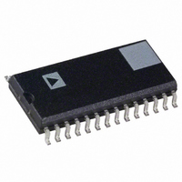
AD9760AR Analog Devices Inc, AD9760AR Datasheet - Page 11

AD9760AR
Manufacturer Part Number
AD9760AR
Description
IC DAC 10BIT 125MSPS 28-SOIC
Manufacturer
Analog Devices Inc
Series
TxDAC®r
Datasheet
1.AD9760ARUZ.pdf
(23 pages)
Specifications of AD9760AR
Mounting Type
Surface Mount
Rohs Status
RoHS non-compliant
Settling Time
35ns
Number Of Bits
10
Number Of Converters
1
Voltage Supply Source
Analog and Digital
Power Dissipation (max)
175mW
Operating Temperature
-40°C ~ 85°C
Package / Case
28-SOIC (7.5mm Width)
Update Rate
125MSPS
Peak Reflow Compatible (260 C)
No
Supply Voltage
5V
No. Of Bits
10 Bit
Leaded Process Compatible
No
Interface Type
Parallel
Resolution
10-Bit
For Use With
AD9760-EBZ - BOARD EVAL FOR AD9760
Data Interface
-
Lead Free Status / RoHS Status
Contains lead / RoHS non-compliant
Available stocks
Company
Part Number
Manufacturer
Quantity
Price
Part Number:
AD9760AR
Manufacturer:
ADI/亚德诺
Quantity:
20 000
Part Number:
AD9760AR50
Manufacturer:
ADI/亚德诺
Quantity:
20 000
Part Number:
AD9760ARU
Manufacturer:
ADI/亚德诺
Quantity:
20 000
Part Number:
AD9760ARU50
Manufacturer:
ADI/亚德诺
Quantity:
20 000
Part Number:
AD9760ARUZ
Manufacturer:
ADI/亚德诺
Quantity:
20 000
Company:
Part Number:
AD9760ARZ-REEL
Manufacturer:
AD
Quantity:
3 400
FUNCTIONAL DESCRIPTION
Figure 39 shows a simplified block diagram of the AD9760.
The AD9760 consists of a large PMOS current source array that
is capable of providing up to 20 mA of total current. The array
is divided into 31 equal currents that make up the 5 most sig-
nificant bits (MSBs). The next 4 bits or middle bits consist
of 15 equal current sources whose value is 1/16th of an MSB
current source. The remaining LSBs is a binary weighted frac-
tion of the middle-bits current sources. Implementing the
middle and lower bits with current sources, instead of an R-2R
ladder, enhances its dynamic performance for multitone or low
amplitude signals and helps maintain the DAC’s high output
impedance (i.e., >100 kΩ).
All of these current sources are switched to one or the other of
the two output nodes (i.e., I
tial current switches. The switches are based on a new architec-
ture that drastically improves distortion performance. This new
switch architecture reduces various timing errors and provides
matching complementary drive signals to the inputs of the dif-
ferential current switches.
The analog and digital sections of the AD9760 have separate
power supply inputs (i.e., AVDD and DVDD) that can operate
independently over a 2.7 volt to 5.5 volt range. The digital
section, which is capable of operating up to a 125 MSPS clock
rate, consists of edge-triggered latches and segment decoding
logic circuitry. The analog section includes the PMOS current
sources, the associated differential switches, a 1.20 V bandgap
voltage reference and a reference control amplifier.
The full-scale output current is regulated by the reference con-
trol amplifier and can be set from 2 mA to 20 mA via an exter-
nal resistor, R
both the reference control amplifier and voltage reference
V
the segmented current sources with the proper scaling factor.
The full-scale current, I
REV. B
REFIO
, sets the reference current I
SET
0.1 F
. The external resistor, in combination with
CLOCK
OUTFS
V
R
REFIO
2k
SET
OUTA
, is thirty-two times the value of I
+5V
I
REF
or I
REF
OUTB
, which is mirrored over to
CLOCK
REFIO
FS ADJ
DVDD
DCOM
SLEEP
+1.20V REF
) via PMOS differen-
REFLO
Figure 39. Functional Block Diagram
SEGMENTED SWITCHES
FOR DB9–DB1
DIGITAL DATA INPUTS (DB9–DB0)
50pF
REF
LATCHES
COMP1
.
CURRENT SOURCE
0.1 F
–11–
ARRAY
PMOS
DAC TRANSFER FUNCTION
The AD9760 provides complementary current outputs, I
and I
I
I
current output appearing at I
both the input code and I
where DAC CODE = 0 to 1023 (i.e., Decimal Representation).
As mentioned previously, I
current I
V
where I
The two current outputs will typically drive a resistive load
directly or via a transformer. If dc coupling is required, I
and I
loads, R
R
I
50 Ω or 75 Ω cable. The single-ended voltage output appearing
at the I
Note the full-scale value of V
the specified output compliance range to maintain specified
distortion and linearity performance.
OUTFS
OUTB
OUTA
+5V
REFIO
LOAD
V
V
AVDD
SWITCH
OUTA
OUTB
I
I
I
LSB
OUTB
OUTA
OUTB
OUTFS
OUTB
, the complementary output, provides no current. The
, when all bits are high (i.e., DAC CODE = 1023) while
or I
may represent the equivalent load resistance seen by
and external resistor R
OUTA
REF
LOAD
= I
REF
= I
. I
OUTB
AD9760
= (DAC CODE/1024) × I
= (1023 – DAC CODE)/1024 × I
should be directly connected to matching resistive
= V
= 32 × I
OUTA
ACOM
OUTA
OUTB
, which is nominally set by a reference voltage,
and I
, that are tied to analog common, ACOM. Note,
COMP2
REFIO
I
as would be the case in a doubly terminated
I
OUTB
OUTA
will provide a near full-scale current output,
× R
× R
OUTB
REF
/R
LOAD
LOAD
0.1 F
SET
I
OUTB
nodes is simply:
OUTFS
OUTFS
I
OUTA
OUTA
OUTA
SET
V
and can be expressed as:
DIFF
V
. It can be expressed as:
R
50
is a function of the reference
OUTB
LOAD
and I
and V
= V
OUTFS
OUTA
OUTB
OUTB
– V
V
R
50
OUTB
OUTFS
OUTA
LOAD
is a function of
should not exceed
AD9760
OUTA
OUTA
(1)
(2)
(3)
(4)
(5)
(6)


