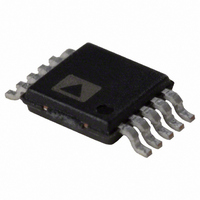
AD5063BRMZ Analog Devices Inc, AD5063BRMZ Datasheet

AD5063BRMZ
Specifications of AD5063BRMZ
Available stocks
Related parts for AD5063BRMZ
AD5063BRMZ Summary of contents
Page 1
FEATURES Single 16-bit DAC, 1 LSB INL Power-on reset to midscale Guaranteed monotonic by design 3 power-down functions Low power serial interface with Schmitt-triggered inputs 10-lead MSOP, low power Fast settling time of 1 μs maximum (AD5063-1 model) 2.7 V ...
Page 2
AD5063 TABLE OF CONTENTS Features .............................................................................................. 1 Applications ....................................................................................... 1 Functional Block Diagram .............................................................. 1 General Description ......................................................................... 1 Product Highlights ........................................................................... 1 Revision History ............................................................................... 2 Specifications ..................................................................................... 3 Timing Characteristics ................................................................ 5 Absolute Maximum Ratings ............................................................ 6 ESD ...
Page 3
... Bipolar Zero Temperature Coefficient Bipolar Gain Error 2 OUTPUT CHARACTERISTICS Output Voltage Range Output Voltage Settling Time 3 AD5063BRMZ AD5063BRMZ-1 Output Noise Spectral Density Output Voltage Noise Digital-to-Analog Glitch Impulse Digital Feedthrough DC Output Impedance (Normal) DC Output Impedance (Power-Down) (Output Connected to 1 kΩ Network) (Output Connected to 10 kΩ ...
Page 4
AD5063 Parameter POWER REQUIREMENTS (Normal Mode (All Power-Down Modes 4 5 ...
Page 5
TIMING CHARACTERISTICS 5.5 V; all specifications T DD Table 3. 1 Parameter Limit ...
Page 6
AD5063 ABSOLUTE MAXIMUM RATINGS Table 4. Parameter V to GND DD Digital Input Voltage to GND V to GND OUT V to GND REF INV to GND R to GND FB Operating Temperature Range Industrial (B Version) Storage Temperature Range ...
Page 7
PIN CONFIGURATION AND FUNCTION DESCRIPTIONS Table 5. Pin Function Descriptions Pin No. Mnemonic Description 1 DIN Serial Data Input. This device has a 24-bit shift register. Data is clocked into the register on the falling edge of the serial clock ...
Page 8
AD5063 TYPICAL PERFORMANCE CHARACTERISTICS 1 25° 4.096V DD REF 1.0 0.8 0.6 0.4 0.2 0 –0.2 –0.4 –0.6 –0.8 –1.0 0 10000 20000 30000 40000 DAC CODE Figure 4. INL Error ...
Page 9
T = 25° MAX INL @ MIN INL @ V = 5.5V DD –1 –2 – REFERENCE VOLTAGE (V) Figure 10. INL Error vs. Reference Input Voltage ...
Page 10
AD5063 1 25° 2.7V 0.9 REF 0.8 0.7 0.6 0.5 0.4 0.3 0.2 0.1 0 2.7 3.2 3.7 4.2 4.7 SUPPLY VOLTAGE (V) Figure 16. Supply Current vs. Supply Voltage 24TH CLOCK FALLING CH1 = ...
Page 11
4.096V DD REF 2.0V 0.008 DD REF 0.006 0.004 0.002 0 GAIN ERROR @ V –0.002 –0.004 –0.006 GAIN ERROR @ V –0.008 –0.010 –40 – ...
Page 12
AD5063 TERMINOLOGY Relative Accuracy For the DAC, relative accuracy, or integral nonlinearity (INL measure of the maximum deviation, in LSB, from a straight line passing through the endpoints of the DAC transfer function. A typical INL error vs. ...
Page 13
THEORY OF OPERATION The AD5063 is a single 16-bit, serial input, voltage-output DAC. It operates from supply voltages of 2 5.5 V. Data is written to the AD5063 in a 24-bit word format via a 3-wire serial interface. ...
Page 14
AD5063 POWER-ON TO MIDSCALE The AD5063 contains a power-on reset circuit that controls the output voltage during power-up. The DAC register is filled with the midscale code, and the output voltage is midscale until a valid write sequence is made ...
Page 15
AD5063 to 68HC11/68L11 Interface Figure 32 shows a serial interface between the AD5063 and the 68HC11/68L11 microcontroller. SCK of the 68HC11/68L11 drives the SCLK pin of the AD5063, and the MOSI output drives the serial data line of the DAC. ...
Page 16
AD5063 APPLICATIONS CHOOSING A REFERENCE FOR THE AD5063 To achieve optimum performance of the AD5063, thought should be given to the choice of a precision voltage reference. The AD5063 has one reference input, V reference input is used to supply ...
Page 17
USING THE AD5063 WITH A GALVANICALLY ISOLATED INTERFACE CHIP In process-control applications in industrial environments often necessary to use a galvanically isolated interface to protect and isolate the controlling circuitry from hazardous common- mode voltages that may occur ...
Page 18
... AD5063 OUTLINE DIMENSIONS ORDERING GUIDE Model Temperature Range 1 AD5063BRMZ −40°C to +85°C 1 AD5063BRMZ-REEL7 −40°C to +85°C 1 AD5063BRMZ-1 −40°C to +85°C 1 AD5063BRMZ-1-REEL7 −40°C to +85°C EVAL-AD5063EB RoHS Compliant Part. 3.10 3.00 2. 5.15 3.10 4.90 3.00 4.65 2. PIN 1 0.50 BSC ...
Page 19
NOTES Rev Page AD5063 ...
Page 20
AD5063 NOTES ©2005–2009 Analog Devices, Inc. All rights reserved. Trademarks and registered trademarks are the property of their respective owners. D04766-0-8/09(C) Rev Page ...


