AD7541AJP-REEL Analog Devices Inc, AD7541AJP-REEL Datasheet - Page 3
AD7541AJP-REEL
Manufacturer Part Number
AD7541AJP-REEL
Description
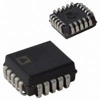
IC DAC 12BIT MULT MONO 20-PLCC
Manufacturer
Analog Devices Inc
Datasheet
1.AD7541AKRZ.pdf
(8 pages)
Specifications of AD7541AJP-REEL
Rohs Status
RoHS non-compliant
Settling Time
600ns
Number Of Bits
12
Data Interface
Parallel
Number Of Converters
1
Voltage Supply Source
Single Supply
Operating Temperature
0°C ~ 70°C
Mounting Type
Surface Mount
Package / Case
20-PLCC
Power Dissipation (max)
-
Available stocks
Company
Part Number
Manufacturer
Quantity
Price
Company:

Part Number:
AD7541AJP-REEL
Manufacturer:
Analog Devices Inc
Quantity:
10 000


ABSOLUTE MAXIMUM RATINGS*
(T
V
CAUTION
ESD (electrostatic discharge) sensitive device. Electrostatic charges as high as 4000 V readily
accumulate on the human body and test equipment and can discharge without detection.
Although the AD7541A features proprietary ESD protection circuitry, permanent damage may
occur on devices subjected to high energy electrostatic discharges. Therefore, proper ESD
precautions are recommended to avoid performance degradation or loss of functionality.
TERMINOLOGY
RELATIVE ACCURACY
Relative accuracy or endpoint nonlinearity is a measure of the
maximum deviation from a straight line passing through the
endpoints of the DAC transfer function. It is measured after
adjusting for zero and full scale and is expressed in % of full-
scale range or (sub)multiples of 1 LSB.
DIFFERENTIAL NONLINEARITY
Differential nonlinearity is the difference between the measured
change and the ideal l LSB change between any two adjacent
codes. A specified differential nonlinearity of 1 LSB max over
the operating temperature range insures monotonicity.
GAIN ERROR
Gain error is a measure of the output error between an ideal
DAC and the actual device output. For the AD7541A, ideal
maximum output is
Gain error is adjustable to zero using external trims as shown in
Figures 4, 5 and 6.
REV. B
V
V
Digital Input Voltage to GND . . . . . . . . –0.3 V, V
OUT 1, OUT 2 to GND . . . . . . . . . . . . –0.3 V, V
Power Dissipation (Any Package)
DD
REF
RFB
BIT 1 (MSB)
To +75 C . . . . . . . . . . . . . . . . . . . . . . . . . . . . . . . 450 mW
Derates above +75 C . . . . . . . . . . . . . . . . . . . . . . 6 mW/ C
A
= +25 C unless otherwise noted)
to GND . . . . . . . . . . . . . . . . . . . . . . . . . . . . . . . . +17 V
to GND . . . . . . . . . . . . . . . . . . . . . . . . . . . . . . . .
to GND . . . . . . . . . . . . . . . . . . . . . . . . . . . . . . . . . 25 V
OUT1
OUT2
BIT 2
BIT 3
BIT 4
BIT 5
BIT 6
GND
1
2
3
4
5
6
7
8
9
(Not to Scale)
AD7541A
TOP VIEW
DIP/SOIC
–
10
18
17
16
15
14
13
12
11
4095
4096
R
V
V
BIT 12 (LSB)
BIT 11
BIT 10
BIT 9
BIT 8
BIT 7
FEEDBACK
REF
DD
(+)
IN
(V
REF
).
NC = NO CONNECT
BIT 1 (MSB)
BIT 2
BIT 3
BIT 4
GND
4
5
6
7
8
DD
DD
PIN CONFIGURATIONS
+ 0.3 V
+ 0.3 V
3
9 10 11 12 13
(Not to Scale)
25 V
AD7541A
TOP VIEW
2
1
LCCC
20 19
–3–
Operating Temperature Range
Storage Temperature . . . . . . . . . . . . . . . . . . –65 C to +150 C
Lead Temperature (Soldering, 10 secs) . . . . . . . . . . . +300 C
*Stresses above those listed under Absolute Maximum Ratings may cause perma-
OUTPUT LEAKAGE CURRENT
Current which appears at OUTI with the DAC loaded to all 0s
or at OUT2 with the DAC loaded to all 1s.
MULTIPLYING FEEDTHROUGH ERROR
AC error due to capacitive feedthrough from V
OUT1 with DAC loaded to all 0s.
OUTPUT CURRENT SETTLING TIME
Time required for the output function of the DAC to settle to
within 1/2 LSB for a given digital input stimulus, i.e., 0 to full
scale.
PROPAGATION DELAY
This is a measure of the internal delay of the circuit and is mea-
sured from the time a digital input changes to the point at which
the analog output at OUT1 reaches 90% of its final value.
DIGITAL-TO-ANALOG CHARGE INJECTION (QDA)
This is a measure of the amount of charge injected from the
digital inputs to the analog outputs when the inputs change
state. It is usually specified as the area of the glitch in nV secs
and is measured with V
output op amp, C1 (phase compensation) = 0 pF.
nent damage to the device. This is a stress rating only; functional operation of the
device at these or any other conditions above those indicated in the operational
sections of this specification is not implied. Exposure to absolute maximum rating
conditions for extended periods may affect device reliability.
Commercial (J, K Versions) . . . . . . . . . . . . . 0 C to +70 C
Industrial (A, B Versions) . . . . . . . . . . . . . –25 C to +85 C
Extended (S, T Versions) . . . . . . . . . . . . . –55 C to +125 C
18
17
16
15
14
V
BIT 12 (LSB)
BIT 11
BIT 10
BIT 9
DD
NC = NO CONNECT
REF
BIT 1 (MSB)
= GND and a Model 50K as the
BIT 2
BIT 3
BIT 4
GND
8
4
5
6
7
WARNING!
9
3
(Not to Scale)
AD7541A
10 11 12 13
TOP VIEW
2
1
PLCC
PIN 1
IDENTIFIER
ESD SENSITIVE DEVICE
AD7541A
20 19
REF
terminal to
18
17
16
14
15
V
BIT 12 (LSB)
BIT 11
BIT 10
BIT 9
DD
Related parts for AD7541AJP-REEL
Image
Part Number
Description
Manufacturer
Datasheet
Request
R

Part Number:
Description:
IC DAC 12BIT MULT MONO 20-PLCC
Manufacturer:
Analog Devices Inc
Datasheet:

Part Number:
Description:
12-Bit/ Multiplying D/A Converter
Manufacturer:
Intersil Corporation
Datasheet:

Part Number:
Description:
±1.7g Dual-Axis IMEMS Accelerometer Evaluation Board
Manufacturer:
Analog Devices Inc
Datasheet:

Part Number:
Description:
Inertial Sensor Evaluation System
Manufacturer:
Analog Devices Inc
Datasheet:
Part Number:
Description:
Manufacturer:
Analog Devices Inc
Datasheet:
Part Number:
Description:
Manufacturer:
Analog Devices Inc
Datasheet:
Part Number:
Description:
Manufacturer:
Analog Devices Inc
Datasheet:
Part Number:
Description:
Manufacturer:
Analog Devices Inc
Datasheet:
Part Number:
Description:
Manufacturer:
Analog Devices Inc
Datasheet:
Part Number:
Description:
Manufacturer:
Analog Devices Inc
Datasheet:
Part Number:
Description:
Manufacturer:
Analog Devices Inc
Datasheet:
Part Number:
Description:
Manufacturer:
Analog Devices Inc
Datasheet:
Part Number:
Description:
Manufacturer:
Analog Devices Inc
Datasheet: