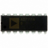
AD7111ABNZ Analog Devices Inc, AD7111ABNZ Datasheet - Page 7

AD7111ABNZ
Manufacturer Part Number
AD7111ABNZ
Description
IC DAC LOGARITHMIC 16-DIP
Manufacturer
Analog Devices Inc
Series
LOGDAC®r
Datasheet
1.AD7111ABRZ.pdf
(8 pages)
Specifications of AD7111ABNZ
Number Of Bits
17
Number Of Converters
1
Voltage Supply Source
Single Supply
Power Dissipation (max)
1W
Operating Temperature
-40°C ~ 85°C
Mounting Type
Through Hole
Package / Case
16-DIP (0.300", 7.62mm)
Resolution (bits)
17bit
Data Interface
Parallel
Supply Voltage Range - Analogue
5V
Supply Current
4mA
Digital Ic Case Style
DIP
No. Of Pins
16
Operating Temperature Range
-40°C To +85°C
Lead Free Status / RoHS Status
Lead free / RoHS Compliant
Settling Time
-
Lead Free Status / RoHS Status
Lead free / RoHS Compliant, Lead free / RoHS Compliant
Available stocks
Company
Part Number
Manufacturer
Quantity
Price
Company:
Part Number:
AD7111ABNZ
Manufacturer:
Analog Devices Inc
Quantity:
135
REV. 0
Typical Performance Characteristics
Another error arises from the output amplifier s input offset
voltage. The amplifier is operated with a fixed feedback resis-
tance, but the equivalent source impedance (the AD7111/
AD7111A output impedance) varies as a function of attenuation
level. This has the effect of varying thc “noise” gain of the
amplifier, thus creating a varying error due to amplifier offset
voltage. It is recommended that an amplifier with less than
50 V of input offset be used (such as the AD OP07 in dc appli-
cations. Amplifiers with higher offset voltage may cause audible
“thumps” in ac applications due to dc output changes.
The AD7111/AD7111A accuracy is specified and tested using
only the internal feedback resistor. Any gain error (i.e., mis-
match of R
Figure 6. Typical Supply Current vs. Logic Input Level
Figure 7. Typical Attenuation Error for 0.75 dB Steps
–0.2
–0.4
–0.6
0.4
0.2
0.0
2
6
5
4
3
1
0
0
FB
*
0
*
* *
to the R-2R ladder) that may exist in the
* * * *
3
* * * *
V
T
A
DD
1
6
= +25 C
* *
= +5V
* * * * * *
9
INPUT VOLTAGE – Volts
ATTENUATION – dB
2
12
CS = WR = 0V
V
T
V
A
DD
* *
IN
= +25 C
APPLIED TO ALL DATA INPUTS
* * *
= +5V
15
* *
3
18
*
* *
* * *
21
* *
4
24
*
*
*
* *
27
*
* *
5
30
*
–7–
AD7111/AD7111A D/A converter circuit results in a constant
attenuation error over the whole range. The AD7111/AD7111A
accuracy is specified relative to 0 dB attenuation, hence “Gain”
trim resistors—R1 and R2 in Figure 1—can be used to adjust
V
00000000. The accuracy and monotonic range specifications of
the AD7111/AD7111A are not affected in any way by this gain
trim procedure. For the AD7111/AD7111A L/C/U grades, suit-
able values for R1 and R2 of Figure 1 are R1 = 500 , R2 =
180 ; for the K/B/T grades, suitable value are R1 = 1000 ,
R2 = 270 . For additional information on gain error the reader
is referred to the “CMOS DAC Application Guide,” available
from Analog Devices, Inc., Publication Number G872b–8–1/89.
Figure 8. Typical Attenuation Error for 3 dB Steps vs.
Temperature
Figure 9. Accuracy Specification for K/B/T Grade Devices
at T
OUT
A
= V
= +25 C
–0.5
–1.0
1.0
0.5
0.0
IN
0
precisely (i.e., 0 dB attenuation) with input code
6
V
DD
12
= +5V
18
24
30
ATTENUATION – dB
36
T
A
AD7111/AD7111A
= +85 C
42
48
54
T
A
= +25 C
60
66
72
78
84


