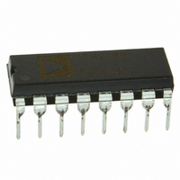
AD7243AN Analog Devices Inc, AD7243AN Datasheet - Page 7

AD7243AN
Manufacturer Part Number
AD7243AN
Description
IC SRL DAC 12BIT LC2MOS 16-DIP
Manufacturer
Analog Devices Inc
Series
DACPORT®r
Datasheet
1.AD7243ANZ.pdf
(12 pages)
Specifications of AD7243AN
Data Interface
Serial
Settling Time
10µs
Rohs Status
RoHS non-compliant
Number Of Bits
12
Number Of Converters
1
Voltage Supply Source
Dual ±
Power Dissipation (max)
100mW
Operating Temperature
-40°C ~ 85°C
Mounting Type
Through Hole
Package / Case
16-DIP (0.300", 7.62mm)
Resolution (bits)
12bit
Digital Ic Case Style
DIP
No. Of Pins
16
Operating Temperature Range
-40°C To +85°C
Update Rate
0.1MSPS
Package
16PDIP
Resolution
12 Bit
Conversion Rate
300 KSPS
Architecture
R-2R
Digital Interface Type
Serial (3-Wire)
Number Of Outputs Per Chip
1
Output Type
Voltage
Full Scale Error
±6 LSB
Integral Nonlinearity Error
±1 LSB
Maximum Settling Time
10 us
Number Of Channels
1
Interface Type
Serial (3-Wire)
Single Supply Voltage (typ)
12/15V
Dual Supply Voltage (typ)
±12/±15V
Power Supply Requirement
Single/Dual
Single Supply Voltage (min)
10.8V
Single Supply Voltage (max)
16.5V
Dual Supply Voltage (min)
±10.8V
Dual Supply Voltage (max)
±16.5V
Operating Temp Range
-40C to 85C
Operating Temperature Classification
Industrial
Mounting
Through Hole
Pin Count
16
Package Type
PDIP
Lead Free Status / Rohs Status
Not Compliant
Available stocks
Company
Part Number
Manufacturer
Quantity
Price
Company:
Part Number:
AD7243AN
Manufacturer:
AD
Quantity:
5 510
Company:
Part Number:
AD7243ANZ
Manufacturer:
AMTEL
Quantity:
648
Part Number:
AD7243ANZ
Manufacturer:
ADI/亚德诺
Quantity:
20 000
Although 16 bits of data are clocked into the input register, only
the latter 12 bits get transferred into the DAC latch. The first 4
bits in the 16 bit stream are don’t cares since their value does
not affect the DAC latch data. Therefore, the data format is 4
don’t cares followed by the 12-bit data word with the LSB as
the last bit in the serial stream.
There are two ways in which the DAC latch and hence the ana-
log output may be updated. The status of the LDAC input is
examined after SYNC is taken low. Depending on its status, one
of two update modes is selected.
If LDAC = 0, then the automatic update mode is selected. In
this mode the DAC latch and analog output are updated auto-
matically when the last bit in the serial data stream is clocked in.
The update thus takes place on the sixteenth falling SCLK edge.
If LDAC = 1, then the automatic update is disabled and the
DAC latch is updated by taking LDAC low any time after the
16-bit data transfer is complete. The update now occurs on the
falling edge of LDAC. Note that the LDAC input must be taken
back high again before the next data transfer is initiated.
Serial Data Loading Format (Daisy-Chain Mode)
By connecting DCEN high the daisy-chain mode is enabled.
This mode of operation is designed for multi-DAC systems
where several AD7243s may be connected in cascade (see Fig-
ure 16). In this mode the internal gating circuitry on SCLK is
disabled, and a serial data output facility is enabled. The inter-
nal gating signal is permanently active (low) so that the SCLK
signal is continuously applied to the input shift register when
SCLK
SYNC
LDAC
SDIN
SDO
*
CLR
= DON'T CARE
t
DB15 (N)*
2
UNDEFINED
t
DB11 (N)
4
MSB
t
1
t
5
DB0 (N)
LSB
t
t
11
10
SYNC is low. The data is clocked into the register on each fall-
ing SCLK edge after SYNC going low. If more than 16 clock
pulses are applied, the data ripples out of the shift register and
appears on the SDO line. By connecting this line to the SDIN
input on the next AD7243 in the chain, a multi-DAC interface
may be constructed. Sixteen SCLK pulses are required for each
DAC in the system. Therefore, the total number of clock cycles
must equal 16N where N is the total number of devices in the
chain. When the serial transfer to all devices is complete, SYNC
should be taken high. This prevents any further data being
clocked into the input register.
A continuous SCLK source may be used if it can be arranged
that SYNC is held low for the correct number of clock cycles.
Alternatively, a burst clock containing the exact number of clock
cycles may be used and SYNC taken high some time later.
When the transfer to all input registers is complete, a common
LDAC signal updates all DAC latches with the lower 12 bits of
data in each input register. All analog outputs are therefore up-
dated simultaneously on the falling edge of LDAC.
Clear Function (CLR)
The clear function bypasses the input shift register and loads the
DAC Latch with all 0s. It is activated by taking CLR low. In all
ranges except the Offset Binary bipolar range (–5 V to +5 V) the
output voltage is reset to 0 V. In the offset binary bipolar range
the output is set to –REFIN. The clear function is especially
useful at power-up as it enables the output to be reset to a
known state.
DB15 (N)*
(N + 1)
DB15*
DB11 (N + 1)
DB11 (N)
MSB
MSB
DB0 (N + 1)
DB0 (N)
LSB
LSB
t
3
t
6
AD7243
t
7
t
9
t
8


