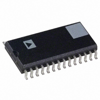
AD9744AR Analog Devices Inc, AD9744AR Datasheet - Page 7

AD9744AR
Manufacturer Part Number
AD9744AR
Description
IC DAC 14BIT 210MSPS 28-SOIC
Manufacturer
Analog Devices Inc
Series
TxDAC®r
Datasheet
1.AD9744ARUZ.pdf
(32 pages)
Specifications of AD9744AR
Rohs Status
RoHS non-compliant
Settling Time
11ns
Number Of Bits
14
Data Interface
Parallel
Number Of Converters
1
Voltage Supply Source
Analog and Digital
Power Dissipation (max)
145mW
Operating Temperature
-40°C ~ 85°C
Mounting Type
Surface Mount
Package / Case
28-SOIC (7.5mm Width)
Number Of Channels
1
Resolution
14b
Interface Type
Parallel
Single Supply Voltage (typ)
3.3V
Dual Supply Voltage (typ)
Not RequiredV
Power Supply Requirement
Analog and Digital
Output Type
Current
Integral Nonlinearity Error
±5LSB
Single Supply Voltage (min)
2.7V
Single Supply Voltage (max)
3.6V
Dual Supply Voltage (min)
Not RequiredV
Dual Supply Voltage (max)
Not RequiredV
Operating Temp Range
-40C to 85C
Operating Temperature Classification
Industrial
Mounting
Surface Mount
Pin Count
28
Package Type
SOIC W
For Use With
AD9744ACP-PCBZ - BOARD EVAL FOR AD9744ACP
Lead Free Status / Rohs Status
Not Compliant
Available stocks
Company
Part Number
Manufacturer
Quantity
Price
Part Number:
AD9744AR
Manufacturer:
ADI/亚德诺
Quantity:
20 000
Part Number:
AD9744ARU
Manufacturer:
ADI/亚德诺
Quantity:
20 000
Part Number:
AD9744ARUZ
Manufacturer:
ADI/亚德诺
Quantity:
20 000
Part Number:
AD9744ARZ
Manufacturer:
ADI/亚德诺
Quantity:
20 000
PIN CONFIGURATIONS AND FUNCTION DESCRIPTIONS
Table 5. Pin Function Descriptions
SOIC/TSSOP
Pin No.
1
2 to 13
14
15
16
17
18
19
20
21
22
23
24
25
N/A
26
27
28
N/A
N/A
N/A
N/A
(MSB) DB13
(LSB) DB0
Figure 3. 28-Lead SOIC and TSSOP
LFCSP
Pin No.
27
28 to 32,
1, 2, 4 to 8
9
25
N/A
23
24
N/A
19, 22
20
21
N/A
17, 18
16
15
10, 26
3
N/A
12
13
11
14
DB12
DB11
DB10
DB9
DB8
DB7
DB6
DB5
DB4
DB3
DB2
DB1
10
11
12
13
14
1
2
3
4
5
6
7
8
9
NC = NO CONNECT
(Not to Scale)
AD9744
TOP VIEW
Mnemonic
DB13
DB12 to
DB1
DB0
SLEEP
REFLO
REFIO
FS ADJ
NC
ACOM
IOUTB
IOUTA
RESERVED
AVDD
MODE
CMODE
DCOM
DVDD
CLOCK
CLK+
CLK−
CLKVDD
CLKCOM
28
27
26
25
24
23
22
21
20
19
18
17
16
15
CLOCK
DVDD
DCOM
MODE
AVDD
RESERVED
IOUTA
IOUTB
ACOM
NC
FS ADJ
REFIO
REFLO
SLEEP
DAC Current Output. Full-scale current when all data bits are 1s.
Reserved. Do not connect to common or supply.
Description
Most Significant Data Bit (MSB).
Data Bits 12 to 1.
Least Significant Data Bit (LSB).
Power-Down Control Input. Active high. Contains active pull-down circuit; it may be left
unterminated if not used.
Reference Ground when Internal 1.2 V Reference Used. Connect to ACOM for both internal
and external reference operation modes.
Reference Input/Output. Serves as reference input when using external reference. Serves as
1.2 V reference output when using internal reference. Requires 0.1 µF capacitor to ACOM
when using internal reference.
Full-Scale Current Output Adjust.
No Internal Connection.
Analog Common.
Complementary DAC Current Output. Full-scale current when all data bits are 0s.
Analog Supply Voltage (3.3 V).
Selects Input Data Format. Connect to DCOM for straight binary, DVDD for twos complement.
Clock Mode Selection. Connect to CLKCOM for single-ended clock receiver (drive CLK+ and
float CLK−). Connect to CLKVDD for differential receiver. Float for PECL receiver (terminations
on-chip).
Digital Common.
Digital Supply Voltage (3.3 V).
Clock Input. Data latched on positive edge of clock.
Differential Clock Input.
Differential Clock Input.
Clock Supply Voltage (3.3 V).
Clock Common.
Rev. B | Page 7 of 32
DVDD 3
DB7 1
DB6 2
DB5 4
DB4 5
DB3 6
DB2 7
DB1 8
NC = NO CONNECT
Figure 4. 32-Lead LFCSP
(Not to Scale)
PIN 1
INDICATOR
AD9744
TOP VIEW
24 FS ADJ
23 REFIO
22 ACOM
21 IOUTA
20 IOUTB
19 ACOM
18 AVDD
17 AVDD
AD9744


