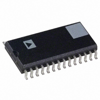
AD9754AR Analog Devices Inc, AD9754AR Datasheet - Page 2

AD9754AR
Manufacturer Part Number
AD9754AR
Description
IC DAC 14BIT 125MSPS HP 28-SOIC
Manufacturer
Analog Devices Inc
Series
TxDAC®r
Datasheet
1.AD9754ARUZ.pdf
(24 pages)
Specifications of AD9754AR
Rohs Status
RoHS non-compliant
Settling Time
35ns
Number Of Bits
14
Data Interface
Parallel
Number Of Converters
1
Voltage Supply Source
Analog and Digital
Power Dissipation (max)
220mW
Operating Temperature
-40°C ~ 85°C
Mounting Type
Surface Mount
Package / Case
28-SOIC (7.5mm Width)
Package
28SOIC W
Resolution
14 Bit
Conversion Rate
125 MSPS
Digital Interface Type
Parallel
Number Of Outputs Per Chip
1
Output Type
Current
Full Scale Error
±5 %FSR
Integral Nonlinearity Error
±3 LSB
Maximum Settling Time
0.035(Typ) us
Available stocks
Company
Part Number
Manufacturer
Quantity
Price
Part Number:
AD9754AR
Manufacturer:
ADI/亚德诺
Quantity:
20 000
Part Number:
AD9754ARU
Manufacturer:
ADI/亚德诺
Quantity:
20 000
Company:
Part Number:
AD9754ARUZ
Manufacturer:
TI
Quantity:
236
Part Number:
AD9754ARUZ
Manufacturer:
ADI/亚德诺
Quantity:
20 000
Part Number:
AD9754ARUZ-REEL7
Manufacturer:
ADI/亚德诺
Quantity:
20 000
AD9754–SPECIFICATIONS
DC SPECIFICATIONS
Parameter
RESOLUTION
DC ACCURACY
ANALOG OUTPUT
REFERENCE OUTPUT
REFERENCE INPUT
TEMPERATURE COEFFICIENTS
POWER SUPPLY
OPERATING RANGE
NOTES
1
2
3
4
5
6
7
Specifications subject to change without notice.
Measured at IOUTA, driving a virtual ground.
Nominal full-scale current, I
Use an external buffer amplifier to drive any external load.
Requires +5 V supply.
Measured at f
Logic level for SLEEP pin must be referenced to AVDD. Min V
5% Power supply variation.
Integral Linearity Error (INL)
Differential Nonlinearity (DNL)
Offset Error
Gain Error (Without Internal Reference)
Gain Error (With Internal Reference)
Full-Scale Output Current
Output Compliance Range
Output Resistance
Output Capacitance
Reference Voltage
Reference Output Current
Input Compliance Range
Reference Input Resistance
Small Signal Bandwidth
Offset Drift
Gain Drift (Without Internal Reference)
Gain Drift (With Internal Reference)
Reference Voltage Drift
Supply Voltages
Analog Supply Current (I
Digital Supply Current (I
Supply Current Sleep Mode (I
Power Dissipation
Power Supply Rejection Ratio
Power Supply Rejection Ratio
T
T
AVDD
DVDD
A
A
= +25 C
= +25 C
CLOCK
= 25 MSPS and I
1
5
(5 V, I
OUTFS
DVDD
, is 32
AVDD
OUTFS
3
2
OUT
(T
7
7
)
)
AVDD
—AVDD
—DVDD
MIN
4
5
= static full scale (20 mA).
the I
= 20 mA)
to T
)
REF
6
MAX
current.
, AVDD = +5 V, DVDD = +5 V, I
IH
= 3.5 V.
Min
14
–3.0
–2.0
–0.02
–2
–5
2.0
–1.0
1.14
0.1
4.5
2.7
–0.4
–0.025
–40
–2–
OUTFS
= 20 mA, unless otherwise noted)
Typ
100
5
1.20
100
1
0.5
0
5.0
5.0
34
3.0
4.0
185
1.5
0.75
0.5
1.5
50
100
50
Max
+3.0
+2.0
+0.02
+2
+5
20.0
1.25
1.26
1.25
5.5
5.5
39
5
8
220
+0.4
+0.025
+85
% of FSR
% of FSR
% of FSR/V
% of FSR/V
Units
Bits
LSB
LSB
% of FSR
mA
V
k
pF
V
nA
V
M
MHz
ppm of FSR/ C
ppm of FSR/ C
ppm of FSR/ C
ppm/ C
V
V
mA
mA
mA
mW
C
REV. A


