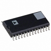
AD9754AR Analog Devices Inc, AD9754AR Datasheet - Page 4

AD9754AR
Manufacturer Part Number
AD9754AR
Description
IC DAC 14BIT 125MSPS HP 28-SOIC
Manufacturer
Analog Devices Inc
Series
TxDAC®r
Datasheet
1.AD9754ARUZ.pdf
(24 pages)
Specifications of AD9754AR
Rohs Status
RoHS non-compliant
Settling Time
35ns
Number Of Bits
14
Data Interface
Parallel
Number Of Converters
1
Voltage Supply Source
Analog and Digital
Power Dissipation (max)
220mW
Operating Temperature
-40°C ~ 85°C
Mounting Type
Surface Mount
Package / Case
28-SOIC (7.5mm Width)
Package
28SOIC W
Resolution
14 Bit
Conversion Rate
125 MSPS
Digital Interface Type
Parallel
Number Of Outputs Per Chip
1
Output Type
Current
Full Scale Error
±5 %FSR
Integral Nonlinearity Error
±3 LSB
Maximum Settling Time
0.035(Typ) us
Available stocks
Company
Part Number
Manufacturer
Quantity
Price
Part Number:
AD9754AR
Manufacturer:
ADI/亚德诺
Quantity:
20 000
Part Number:
AD9754ARU
Manufacturer:
ADI/亚德诺
Quantity:
20 000
Company:
Part Number:
AD9754ARUZ
Manufacturer:
TI
Quantity:
236
Part Number:
AD9754ARUZ
Manufacturer:
ADI/亚德诺
Quantity:
20 000
Part Number:
AD9754ARUZ-REEL7
Manufacturer:
ADI/亚德诺
Quantity:
20 000
ABSOLUTE MAXIMUM RATINGS*
Parameter
AVDD
DVDD
ACOM
AVDD
CLOCK, SLEEP
Digital Inputs
IOUTA, IOUTB
ICOMP
REFIO, FSADJ
REFLO
Junction Temperature
Storage Temperature
Lead Temperature
*Stresses above those listed under Absolute Maximum Ratings may cause perma-
AD9754
DIGITAL SPECIFICATIONS
Parameter
DIGITAL INPUTS
NOTES
1
Specifications subject to change without notice.
CAUTION
ESD (electrostatic discharge) sensitive device. Electrostatic charges as high as 4000 V readily
accumulate on the human body and test equipment and can discharge without detection.
Although the AD9754 features proprietary ESD protection circuitry, permanent damage may
occur on devices subjected to high energy electrostatic discharges. Therefore, proper ESD
precautions are recommended to avoid performance degradation or loss of functionality.
When DVDD = +5 V and Logic 1 voltage 3.5 V and Logic 0 voltage
nent damage to the device. This is a stress rating only; functional operation of the
device at these or any other conditions above those indicated in the operational
sections of this specification is not implied. Exposure to absolute maximum ratings
for extended periods may affect device reliability.
(10 sec)
Logic “1” Voltage @ DVDD = +5 V
Logic “1” Voltage @ DVDD = +3 V
Logic “0” Voltage @ DVDD = +5 V
Logic “0” Voltage @ DVDD = +3 V
Logic “1” Current
Logic “0” Current
Input Capacitance
Input Setup Time (t
Input Hold Time (t
Latch Pulsewidth (t
H
LPW
S
With
Respect to
ACOM
DCOM
DCOM
DVDD
DCOM
DCOM
ACOM
ACOM
ACOM
ACOM
)
)
)
DB0–DB11
Min
–0.3
–0.3
–0.3
–6.5
–0.3
–0.3
–1.0
–0.3
–0.3
–0.3
–65
CLOCK
IOUTA
IOUTB
1
1
(T
OR
MIN
Max
+6.5
+6.5
+0.3
+6.5
DVDD + 0.3
DVDD + 0.3
AVDD + 0.3
AVDD + 0.3
AVDD + 0.3
AVDD +0.3
+150
+150
+300
to T
MAX
, AVDD = +5 V, DVDD = +5 V, I
Figure 1. Timing Diagram
t
S
Units
V
V
V
V
V
V
V
V
V
V
C
C
C
V IVDD can increase by up to 10 mA depending on f
t
PD
–4–
Model
AD9754AR
AD9754ARU –40 C to +85 C
AD9754-EB
*R = Small Outline IC; RU = Thin Shrink Small Outline Package.
THERMAL CHARACTERISTICS
Thermal Resistance
28-Lead 300 Mil SOIC
28-Lead TSSOP
0.1%
t
t
ST
JA
JC
JA
JC
Min
3.5
2.1
–10
–10
2.0
1.5
3.5
LPW
= 71.4 C/W
= 97.9 C/W
= 23 C/W
= 14.0 C/W
t
H
OUTFS
0.1%
Temperature
Range
–40 C to +85 C 28-Lead 300 Mil SOIC R-28
= 20 mA unless otherwise noted)
Typ
5
3
0
0
5
ORDERING GUIDE
Evaluation Board
Package
Descriptions
28-Lead TSSOP
WARNING!
CLOCK
Max
1.3
0.9
+10
+10
.
ESD SENSITIVE DEVICE
Package
Options*
RU-28
Units
V
V
V
V
pF
ns
ns
ns
REV. A
A
A


