AD7224LP Analog Devices Inc, AD7224LP Datasheet - Page 5
AD7224LP
Manufacturer Part Number
AD7224LP
Description
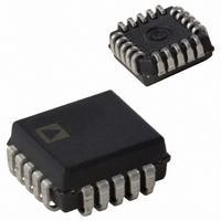
IC DAC 8BIT LC2MOS W/AMP 20PLCC
Manufacturer
Analog Devices Inc
Datasheet
1.AD7224KRZ-1.pdf
(8 pages)
Specifications of AD7224LP
Rohs Status
RoHS non-compliant
Settling Time
7µs
Number Of Bits
8
Data Interface
Parallel
Number Of Converters
1
Voltage Supply Source
Dual ±
Power Dissipation (max)
75mW
Operating Temperature
-40°C ~ 85°C
Mounting Type
Surface Mount
Package / Case
20-PLCC
Available stocks
Company
Part Number
Manufacturer
Quantity
Price

Part Number:
AD7224LP
Manufacturer:
ADI/亚德诺
Quantity:
20 000
Company:
Part Number:
AD7224LP-REEL
Manufacturer:
Analog Devices Inc
Quantity:
10 000
Part Number:
AD7224LP-REEL
Manufacturer:
ADI/亚德诺
Quantity:
20 000
Company:
Part Number:
AD7224LPZ
Manufacturer:
Analog Devices Inc
Quantity:
10 000


REV. B
TERMINOLOGY
TOTAL UNADJUSTED ERROR
Total Unadjusted Error is a comprehensive specification which
includes full-scale error, relative accuracy and zero code error.
Maximum output voltage is V
(ideal) is V
Hence the zero code error, relative to the LSB size, will increase
as V
which includes the zero code error, will also vary in terms of
LSBs over the V
specified for a fixed reference voltage of +10 V.
RELATIVE ACCURACY
Relative Accuracy or endpoint nonlinearity is a measure of the
maximum deviation from a straight line passing through the
endpoints of the DAC transfer function. It is measured after al-
lowing for zero code error and full-scale error and is normally
expressed in LSBs or as a percentage of full-scale reading.
DIFFERENTIAL NONLINEARITY
Differential Nonlinearity is the difference between the measured
change and the ideal 1 LSB change between any two adjacent
codes. A specified differential nonlinearity of 1 LSB max over
the operating temperature range ensures monotonicity.
DIGITAL FEEDTHROUGH
Digital Feedthrough is the glitch impulse transferred to the out-
put due to a change in the digital input code. It is specified in
nV secs and is measured at V
FULL-SCALE ERROR
Full-Scale Error is defined as:
CIRCUIT INFORMATION
D/A SECTION
The AD7224 contains an 8-bit voltage-mode digital-to-analog
converter. The output voltage from the converter has the same
polarity as the reference voltage, allowing single supply opera-
tion. A novel DAC switch pair arrangement on the AD7224 al-
lows a reference voltage range from +2 V to +12.5 V.
The DAC consists of a highly stable, thin-film, R-2R ladder and
eight high speed NMOS single pole, double-throw switches.
The simplified circuit diagram for this DAC is shown in
Figure 1.
The input impedance at the V
vary from 8 k minimum to infinity. The lowest input imped-
ance occurs when the DAC is loaded with the digital code
01010101. Therefore, it is important that the reference presents
a low output impedance under changing load conditions. The
nodal capacitance at the reference terminals is also code depen-
dent and typically varies from 25 pF to 50 pF.
The V
voltage source with an output voltage of:
AGND
Measured Value – Zero Code Error – Ideal Value
V
REF
REF
OUT
decreases. Accordingly, the total unadjusted error,
2R
Figure 1. D/A Simplified Circuit Diagram
pin can be considered as a digitally programmable
REF
/256. The LSB size will vary over the V
DB0
2R
REF
R
range. As a result, total unadjusted error is
DB0
2R
R
REF
REF
REF
DB0
= 0 V.
2R
– 1 LSB (ideal), where 1 LSB
pin is code dependent and can
R
DB0
2R
SHOWN FOR ALL 1's ON DAC
V
REF
OUT
range.
–5–
OP-AMP SECTION
The voltage-mode D/A converter output is buffered by a unity
gain noninverting CMOS amplifier. This buffer amplifier is
capable of developing +10 V across a 2 k load and can drive
capacitive loads of 3300 pF.
The AD7224 can be operated single or dual supply resulting in
different performance in some parameters from the output am-
plifier. In single supply operation (V
capability of the amplifier, which is normally 400 A, is reduced
as the output voltage nears AGND. The full sink capability of
400 A is maintained over the full output voltage range by tying
V
Settling-time for negative-going output signals approaching
AGND is similarly affected by V
for single supply operation is longer than for dual supply opera-
tion. Positive-going settling-time is not affected by V
Additionally, the negative V
put amplifier which results in better zero code performance and
improved slew-rate at the output, than can be obtained in the
single supply mode.
DIGITAL SECTION
The AD7224 digital inputs are compatible with either TTL or
5 V CMOS levels. All logic inputs are static-protected MOS
gates with typical input currents of less than 1 nA. Internal in-
put protection is achieved by an on-chip distributed diode be-
tween DGND and each MOS gate. To minimize power supply
currents, it is recommended that the digital input voltages be
driven as close to the supply rails (V
cally possible.
INTERFACE LOGIC INFORMATION
Table I shows the truth table for AD7224 operation. The part
contains two registers, an input register and a DAC register. CS
and WR control the loading of the input register while LDAC
and WR control the transfer of information from the input regis-
ter to the DAC register. Only the data held in the DAC register
will determine the analog output of the converter.
All control signals are level-triggered and therefore either or
both registers may be made transparent; the input register by
keeping CS and WR “LOW”, the DAC register by keeping
LDAC and WR “LOW”. Input data is latched on the rising
edge of WR.
SS
where D is a fractional representation of the digital input code
and can vary from 0 to 255/256.
to –5 V. This is indicated in Figure 2.
Figure 2. Variation of I
500
400
300
200
100
0
0
V
V
SS
SS
2
V
= 0V
= –5V
OUT
SS
gives more headroom to the out-
V
= D • V
4
OUT
SS
. Negative-going settling-time
– Volts
SS
DD
SINK
6
REF
= 0 V = AGND) the sink
and DGND) as practi-
V
T
with V
A
DD
= 25 C
= +15V
8
AD7224
OUT
10
SS
.
Related parts for AD7224LP
Image
Part Number
Description
Manufacturer
Datasheet
Request
R

Part Number:
Description:
±1.7g Dual-Axis IMEMS Accelerometer Evaluation Board
Manufacturer:
Analog Devices Inc
Datasheet:

Part Number:
Description:
Inertial Sensor Evaluation System
Manufacturer:
Analog Devices Inc
Datasheet:
Part Number:
Description:
Manufacturer:
Analog Devices Inc
Datasheet:
Part Number:
Description:
Manufacturer:
Analog Devices Inc
Datasheet:
Part Number:
Description:
Manufacturer:
Analog Devices Inc
Datasheet:
Part Number:
Description:
Manufacturer:
Analog Devices Inc
Datasheet:
Part Number:
Description:
Manufacturer:
Analog Devices Inc
Datasheet:
Part Number:
Description:
Manufacturer:
Analog Devices Inc
Datasheet:
Part Number:
Description:
Manufacturer:
Analog Devices Inc
Datasheet:
Part Number:
Description:
Manufacturer:
Analog Devices Inc
Datasheet:
Part Number:
Description:
Manufacturer:
Analog Devices Inc
Datasheet:
Part Number:
Description:
Manufacturer:
Analog Devices Inc
Datasheet:
Part Number:
Description:
Manufacturer:
Analog Devices Inc
Datasheet: