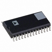
AD7805CR Analog Devices Inc, AD7805CR Datasheet - Page 18

AD7805CR
Manufacturer Part Number
AD7805CR
Description
IC DAC 10BIT QUAD PARALL 28-SOIC
Manufacturer
Analog Devices Inc
Datasheet
1.AD7808BRZ.pdf
(28 pages)
Specifications of AD7805CR
Rohs Status
RoHS non-compliant
Settling Time
1.5µs
Number Of Bits
10
Data Interface
Parallel
Number Of Converters
4
Voltage Supply Source
Analog and Digital
Power Dissipation (max)
66mW
Operating Temperature
-40°C ~ 85°C
Mounting Type
Surface Mount
Package / Case
28-SOIC (7.5mm Width)
Available stocks
Company
Part Number
Manufacturer
Quantity
Price
Part Number:
AD7805CR
Manufacturer:
ADI/亚德诺
Quantity:
20 000
AD7804/AD7805/AD7808/AD7809
Table VI and Figure 22 show the analog outputs available for
the above configuration. The following is the procedure re-
quired if the complete transfer function needs to be offset
around the V
log output variations available from the Sub DAC.
System Control Register Write:
Channel Control Register Write:
DAC Data Register Write:
Channel Control Register Write:
DAC Data Register Write:
MODE = 0, address inputs (A2, A1, A0) are don’t cares.
MODE = 0, address inputs (A2, A1, A0) select desired channel.
MODE = 1, address inputs (A2, A1, A0) select desired channel.
MODE = 0, address inputs (A2, A1, A0) select desired channel.
MODE = 1, address inputs (A2, A1, A0) select desired channel.
Write 020 Hex
Write 091 Hex
Write XX Hex
Write 011 Hex
Write XXX Hex With MODE = 1 all data writes are to
BIAS
point. Table VII and Figure 23 show the ana-
Configure part for 10-bit parallel, twos
complement coding, normal operation
Internal V
DAC, and any DAC data writes that
follow are to the Sub DAC.
With MODE = 1 all data writes are to
the selected DACs Sub DAC. XX is the
required data. 7F Hex will give zero scale
and 80 Hex will give full scale from the
Sub DAC.
Internal V
DAC, and any DAC data writes that
follow are to the Main DAC.
the selected Main DAC. XXX is the
required data. 1FF Hex will give zero
scale and 200 Hex will give full scale
from the DAC.
DD
DD
/2 selected as V
/2 selected as V
BIAS
BIAS
for
for
–18–
OFFSET BINARY CODING
Table VIII shows the offset binary transfer function for the Main
DAC.
Digital Inputs
MSB . . . LSB
1111111111
1111111110
1000000001
1000000000
0111111111
0000000001
0000000000
NOTE: The span range is (30/16)
Figure 25. Main DAC Output Voltage vs. DAC Input Codes
(HEX) for Offset Binary Coding
Figure 25 shows the Main DAC transfer function when offset
binary coding is used. With offset binary coding selected the
output voltage can be calculated as follows:
where NA is the decimal equivalent of the offset binary input
code. NA ranges from 0 to 1023.
Table IX shows the offset binary transfer function for the Sub
DAC. Figure 26 shows the Sub DAC transfer function for
offset binary coding. Any Sub DAC output voltage can be
expressed as:
where NB is the decimal equivalent of the offset binary input
code. NB ranges from 0 to 255.
V
V
OUT
OUT
DAC INPUT CODE
Table VIII. Offset Binary Code Table for Main DAC
' = V
" = V
BIAS
BIAS
31
16
V
V
V
BIAS
BIAS
BIAS
16
/16
+ 1.875
000
[(NB-128)/256]
001
Analog Output
V
V
V
V
V
V
V
BIAS
BIAS
BIAS
BIAS
BIAS
BIAS
BIAS
V
BIAS
V
+1.875
+1.875
+1.875
+1.875
+1.875
/16
BIAS
= 1.875
1FF 200 201
((NA-512)/1024)
V
V
V
V
V
BIAS
BIAS
BIAS
BIAS
BIAS
V
BIAS
(1023–512)/1024
(1022–512)/1024
/1024
(511–512)/1024
(1–512)/1024
3FE
REV. A
3FF


