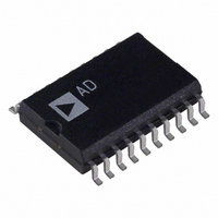
DAC8562FS Analog Devices Inc, DAC8562FS Datasheet - Page 10

DAC8562FS
Manufacturer Part Number
DAC8562FS
Description
IC DAC 12BIT PARALLEL 5V 20-SOIC
Manufacturer
Analog Devices Inc
Datasheet
1.DAC8562FSZ.pdf
(16 pages)
Specifications of DAC8562FS
Rohs Status
RoHS non-compliant
Settling Time
16µs
Number Of Bits
12
Data Interface
Parallel
Number Of Converters
1
Voltage Supply Source
Single Supply
Power Dissipation (max)
30mW
Operating Temperature
-40°C ~ 85°C
Mounting Type
Surface Mount
Package / Case
20-SOIC (7.5mm Width)
Available stocks
Company
Part Number
Manufacturer
Quantity
Price
Part Number:
DAC8562FS
Manufacturer:
ADI/亚德诺
Quantity:
20 000
Company:
Part Number:
DAC8562FS-REEL
Manufacturer:
HIT
Quantity:
183
Part Number:
DAC8562FS-REEL
Manufacturer:
ADI/亚德诺
Quantity:
20 000
Part Number:
DAC8562FSZ
Manufacturer:
ADI/亚德诺
Quantity:
20 000
DAC8562
Unipolar Output Operation
This is the basic mode of operation for the DAC8562. As shown
in Figure 30, the DAC8562 has been designed to drive loads as
low as 820
eration is shown in Table III.
Hexadecimal Number
in DAC Register
FFF
801
800
7FF
000
Operating the DAC8562 on +12 V or +15 V Supplies Only
Although the DAC8562 has been specified to operate on a
single, +5 V supply, a single +5 V supply may not be available in
many applications. Since the DAC8562 consumes no more than
6 mA, maximum, then an integrated voltage reference, such as
the REF02, can be used as the DAC8562 +5 V supply. The
configuration of the circuit is shown in Figure 31. Notice that
the reference’s output voltage requires no trimming because of
the REF02’s excellent load regulation and tight initial output
voltage tolerance. Although the maximum supply current of the
DAC8562 is 6 mA, local bypassing of the REF02’s output with
at least 0. 1 F at the DAC’s voltage supply pin is recommended
to prevent the DAC’s internal digital circuits from affecting the
DAC’s internal voltage reference.
CLR
CE
DATA
Figure 30. Unipolar Output Operation
16
15
in parallel with 500 pF. The code table for this op-
0.1µF
Table III. Unipolar Code Table
DGND
DAC-8562
10
+5V
V
20
DD
AGND
12
10µF
Decimal Number
in DAC Register
4095
2049
2048
2047
0
13
820
0V
500pF
V
OUT
Analog Output
Voltage (V)
+2.047
0
+4.095
+2.049
+2.048
4.095V
–10–
Measuring Offset Error
One of the most commonly specified endpoint errors associated
with real-world nonideal DACs is offset error.
In most DAC testing, the offset error is measured by applying
the zero-scale code and measuring the output deviation from
0 volt. There are some DACs where offset errors may be present
but not observable at the zero scale because of other circuit limi-
tations (for example, zero coinciding with single supply ground).
In these DACs, nonzero output at zero code cannot be read as
the offset error. In the DAC8562, for example, the zero-scale er-
ror is specified to be +3 LSBs. Since zero scale coincides with
zero volt, it is not possible to measure negative offset error.
By adding a pull-down resistor from the output of the
DAC8562 to a negative supply as shown in Figure 32, offset er-
rors can now be read at zero code. This configuration forces the
output P-channel MOSFET to source current to the negative
supply thereby allowing the designer to determine in which di-
rection the offset error appears. The value of the resistor should
be such that, at zero code, current through the resistor is 200 A
maximum.
Figure 31. Operating the DAC8562 on +12 V or +15 V
Supplies Using a REF02 Voltage Reference
Figure 32. Measuring Zero-Scale or Offset Error
CLR
+12V OR +15V
REF-02
CE
DATA
4
2
16
15
0.1µF
DGND
6
DAC-8562
CLR
10
CE
DATA
+5V
V
20
DD
AGND
16
15
12
0.1µF
DGND
13
DAC-8562
10
1
V–
AGND
12
0.1µF
200µA MAX
13
V
V
OUT
OUT
REV. A


