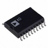
DAC8562FS Analog Devices Inc, DAC8562FS Datasheet - Page 14

DAC8562FS
Manufacturer Part Number
DAC8562FS
Description
IC DAC 12BIT PARALLEL 5V 20-SOIC
Manufacturer
Analog Devices Inc
Datasheet
1.DAC8562FSZ.pdf
(16 pages)
Specifications of DAC8562FS
Rohs Status
RoHS non-compliant
Settling Time
16µs
Number Of Bits
12
Data Interface
Parallel
Number Of Converters
1
Voltage Supply Source
Single Supply
Power Dissipation (max)
30mW
Operating Temperature
-40°C ~ 85°C
Mounting Type
Surface Mount
Package / Case
20-SOIC (7.5mm Width)
Available stocks
Company
Part Number
Manufacturer
Quantity
Price
Part Number:
DAC8562FS
Manufacturer:
ADI/亚德诺
Quantity:
20 000
Company:
Part Number:
DAC8562FS-REEL
Manufacturer:
HIT
Quantity:
183
Part Number:
DAC8562FS-REEL
Manufacturer:
ADI/亚德诺
Quantity:
20 000
Part Number:
DAC8562FSZ
Manufacturer:
ADI/亚德诺
Quantity:
20 000
DAC8562
Decoding Multiple DAC8562s
The CE function of the DAC8562 can be used in applications
to decode a number of DACs. In this application, all DACs re-
ceive the same input data; however, only one of the DACs’ CE
input is asserted to transfer its parallel input register contents
into the DAC. In this circuit, shown in Figure 40, the CE tim-
ing is generated by a 74HC139 decoder and should follow the
DAC8562’s standard timing requirements. To prevent timing
errors, the 74HC139 should not be activated by its ENABLE
input while the coded address inputs are changing. A simple
timing circuit, R1 and C1, connected to the DACs’ CLR pins
resets all DAC outputs to zero during power-up.
MICROPROCESSOR INTERFACING
DAC-8562–MC68HC11 INTERFACE
The circuit illustrated in Figure 41 shows a parallel interface be-
tween the DAC8562 and a popular 8-bit microcontroller, the
M68HC11, which is configured in a single-chip operating
mode. The interface circuit consists of a pair of 74ACT11373
transparent latches and an inverter. The data is loaded into the
latches in two 8-bit bytes; the first byte contains the four most
significant bits, and the lower 8 bits are in the second byte. Data
is taken from the microcontroller’s port B output lines, and
three interface control lines, CLR, CE, and MSB/LSB, are con-
trolled by the M68HC11's PC2, PC1, and PC0 output lines, re-
spectively. To transfer data into the DAC, PC0 is set, enabling
U1’s outputs. The first data byte is loaded into U1 where the
four least significant bits of the byte are connected to
MSB–DB8. PC0 is then cleared; this latches U1’s inputs and
enables U2’s outputs. U2s outputs now become DB7–DB0.
The DAC output is updated with the contents of U1 and U2
*M6BHC11
PC2
PC0
PB7
PB6
PB5
PB4
PB3
PB2
PB0
PC1
PB1
MSB/ LSB
Figure 41. DAC8562 to MC68HC11 Interface
CLR
CE
1
74HC04
2
23
20
23
20
22
16
15
24
22
16
15
24
13
21
1
14
13
21
14
1
74ACT11373
74ACT11373
1D
1D
4D
5D
6D
7D
8D
OC
4D
5D
6D
7D
8D
OC
C
2D
3D
C
2D
3D
–14–
U1
U2
*ADDITIONAL PINS OMITTED FOR CLARITY
when PC1 is cleared. The DAC’s CLR input, controlled by the
M68HC11’s PC2 output line, provides an asynchronous clear
function that sets the DAC’s output to zero. Included in this sec-
tion is the source code for operating the DAC-8562–M68HC11
interface.
1Q
2Q
3Q
4Q
5Q
6Q
7Q
8Q
1Q
2Q
3Q
4Q
5Q
6Q
7Q
8Q
ADDRESS
Figure 40. Decoding Multiple DAC8562s Using the CE Pin
ENABLE
+5V
CODED
10
11
10
11
12
1
12
1
3
4
9
3
4
9
2
2
0.1µF
1k
NC
NC
NC
NC
DATA
+5V
16
15
14
13
1
2
3
PC2
PC1
8
1G
1A
2A
2B
1B
2G
GND
V
CC
74HC139
19
17
15
16
18
2
9
8
7
3
6
5
4
1
*DAC-8562
CE
CLR
MSB
DB10
DB9
DB8
DB7
DB6
DB5
DB4
DB3
DB2
DB1
LSB
1Y0
1Y2
1Y3
2Y0
2Y1
2Y2
1Y1
2Y3
U3
V
OUT
11
10
12
4
5
6
7
9
13
NC
NC
NC
NC
0.1µF
C1
+5V
R1
1k
15
16
15
16
15
16
15
16
DAC-8562
DAC-8562
DAC-8562
DAC-8562
#2
#1
#3
#4
REV. A
13
13
13
13
V
V
V
V
OUT1
OUT2
OUT3
OUT4


