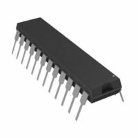
AD7538JNZ Analog Devices Inc, AD7538JNZ Datasheet

AD7538JNZ
Specifications of AD7538JNZ
Available stocks
Related parts for AD7538JNZ
AD7538JNZ Summary of contents
Page 1
FEATURES All grades 14-bit monotonic over the full temperature range Low cost, 14-bit upgrade for 12-bit systems 14-bit parallel load with double buffered inputs Small 24-pin, 0.30” DIP and SOIC Low output leakage (<20 nA) over the full temperature range ...
Page 2
AD7538 TABLE OF CONTENTS Features .............................................................................................. 1 Applications ....................................................................................... 1 Functional Block Diagram .............................................................. 1 General Description ......................................................................... 1 Product Highlights ........................................................................... 1 Revision History ............................................................................... 2 Specifications ..................................................................................... 3 AC Performance Characteristics ................................................ 4 Timing Characteristics ................................................................ 4 Timing ...
Page 3
SPECIFICATIONS 11 15. REF Table Parameter Versions ACCURACY Resolution 14 Relative Accuracy ±2 Differential Nonlinearity ±1 Full-Scale Error +25°C ± ...
Page 4
AD7538 AC PERFORMANCE CHARACTERISTICS These characteristics are included for design guidance only and are not subject to test −300 mV, output amplifier is SS Table Parameter T A Output ...
Page 5
TIMING DIAGRAM LDAC DATA NOTES 1. ALL INPUT SIGNAL RISE AND FALL TIMES MEASURES FROM 10 90 20ns ...
Page 6
AD7538 ABSOLUTE MAXIMUM RATINGS T = +25°C unless, otherwise stated. A Table 4. Parameter V (Pin 23) to DGND DD V (Pin 24) to AGND SS V (Pin 1) to AGND REF V (Pin 2) to AGND RFB Digital Input ...
Page 7
PIN CONFIGURATION AND FUNCTION DESCRIPTIONS Table 5. Pin Function Description Pin No. Mnemonic Description 1 V Voltage Reference. REF 2 R Feedback Resistor. Used to close the loop around an external op amp Current Output Terminal. OUT ...
Page 8
AD7538 TERMINOLOGY Relative Accuracy Relative accuracy or endpoint nonlinearity is a measure of the maximum deviation from a straight line passing through the endpoints of the DAC transfer function measured after adjusting for zero error and full-scale error ...
Page 9
DAC SECTION Figure 4 shows a simplified circuit diagram for the AD7538 DAC section. The three MSBs of the 14-bit data word are decoded to drive the seven switches (A to G). The 11 LSBs of the data word consist ...
Page 10
AD7538 CIRCUIT INFORMATION EQUIVALENT CIRCUIT ANALYSIS Figure 5 shows an equivalent circuit for the analog section of the AD7538 DAC. The current source I of surface and junction leakages. The R equivalent output resistance of the DAC, which varies with ...
Page 11
BIPOLAR OPERATION (4-QUADRANT MULTIPLICATION) The recommended circuit diagram for bipolar operation is shown in Figure 8. Offset binary coding is used. The code table for Figure 8 is given in Table 7. With the DAC loaded to 10 0000 0000 ...
Page 12
AD7538 PROGRAMMABLE GAIN AMPLIFIER The circuit shown in Figure 9 provides a programmable gain amplifier (PGA the DAC behaves as a programmable resistance and thus allows the circuit gain to be digitally controlled. DIGITAL INPUT ...
Page 13
APPLICATION HINTS OUTPUT OFFSET CMOS DACs in circuits such as Figure 6 and Figure 8 exhibit a code dependent output resistance, which in turn can cause a code dependent error voltage at the output of the amplifier. The maximum amplitude ...
Page 14
AD7538 DIGITAL FEEDTHROUGH The digital inputs to the AD7538 are directly connected to the microprocessor bus in the preceding interface configurations. These inputs are constantly changing even when the device is not selected. The high frequency logic activity on the ...
Page 15
OUTLINE DIMENSIONS 24 1 0.210 (5.33) MAX 0.150 (3.81) 0.130 (3.30) 0.115 (2.92) 0.022 (0.56) 0.018 (0.46) 0.014 (0.36) CONTROLLING DIMENSIONS ARE IN INCHES; MILLIMETER DIMENSIONS (IN PARENTHESES) ARE ROUNDED-OFF INCH EQUIVALENTS FOR REFERENCE ONLY AND ARE NOT APPROPRIATE FOR ...
Page 16
... AD7538 0.30 (0.0118) 0.10 (0.0039) COPLANARITY 0.10 ORDERING GUIDE Model Temperature Range AD7538JN 0°C to +70°C 1 AD7538JNZ 0°C to +70°C AD7538KN 0°C to +70°C 1 AD7538KNZ 0°C to +70°C AD7538JR 0°C to +70°C AD7538JR-REEL 0°C to +70°C AD7538JRZ 1 0°C to +70°C ...


