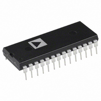
AD667JN Analog Devices Inc, AD667JN Datasheet - Page 3

AD667JN
Manufacturer Part Number
AD667JN
Description
IC DAC 12BIT V-OUT 28-DIP
Manufacturer
Analog Devices Inc
Datasheet
1.AD667JNZ.pdf
(8 pages)
Specifications of AD667JN
Settling Time
3µs
Rohs Status
RoHS non-compliant
Number Of Bits
12
Number Of Converters
1
Voltage Supply Source
Dual ±
Power Dissipation (max)
1W
Operating Temperature
0°C ~ 70°C
Mounting Type
Through Hole
Package / Case
28-DIP (0.600", 15.24mm)
Resolution (bits)
12bit
Data Interface
CMOS, Byte, Nibble, Parallel, TTL
Digital Ic Case Style
DIP
No. Of Pins
28
Operating Temperature Range
0°C To +70°C
Update Rate
0.5MSPS
Package
28PDIP W
Resolution
12 Bit
Conversion Rate
500 KSPS
Architecture
Current Steering
Digital Interface Type
Parallel
Number Of Outputs Per Chip
1
Output Type
Voltage
Full Scale Error
±0.2 %FSR
Integral Nonlinearity Error
±0.75 LSB
Maximum Settling Time
4 us
Lead Free Status / RoHS Status
Contains lead / RoHS non-compliant
Available stocks
Company
Part Number
Manufacturer
Quantity
Price
Part Number:
AD667JN
Manufacturer:
ADI/亚德诺
Quantity:
20 000
Company:
Part Number:
AD667JNZ
Manufacturer:
PSPR
Quantity:
6 220
Part Number:
AD667JNZ
Manufacturer:
ADI/亚德诺
Quantity:
20 000
Model
DIGITAL INPUTS
TRANSFER CHARACTERISTICS
DRIFT
CONVERSION SPEED
ANALOG OUTPUT
REFERENCE OUTPUT
POWER SUPPLY SENSITIVITY
POWER SUPPLY REQUIREMENTS
TEMPERATURE RANGE
TIMING DIAGRAMS
WRITE CYCLE #1
(Load First Rank from Data Bus; A3 = 1)
REV. A
Resolution
Logic Levels (TTL, Compatible, T
V
V
I
I
ACCURACY
Differential Linearity
Gain (Full Scale) T
Unipolar Offset T
Bipolar Zero T
Settling Time to 0.01% of FSR for
Ranges
Output Current
Output Impedance (DC)
Short Circuit Current
External Current
V
V
Rated Voltages
Range
Supply Current
Specification
Storage
IH
IL
IH
IL
CC
EE
Linearity Error @ +25 C
Differential Linearity Error @ +25 C
Gain Error
Unipolar Offset Error
Bipolar Zero
FSR Change (2 k
For LSB Change
+11.4 V to +16.5 V dc
–11.4 V to –16.5 V dc
(V
(V
(Logic “0”)
(Logic “l’’)
= –11.4 V to –16.5 V dc
= +11.4 V to +16.5 V dc
T
T
with 10 k Feedback
with 5 k Feedback
Slew Rate
IL
IH
4
A
A
4
= 0.8 V)
= 5.5 V)
= T
= T
MIN
MIN
2
A
2
to T
to T
= 25 C to T
A
A
= 25 C to T
= 25 C to T
MAX
MAX
500 pF Load)
2
MIN
MIN
MIN
MIN
or T
or T
or T
–T
MAX
MAX
MAX
MAX
)
1
Min
+2.0
0
Monotonicity Guaranteed
10
9.90
0.1
–25
–65
5
11.4
AD667A
Typ
3
1
+1/4
3
2
1
+5, +10
0.05
10.00
1.0
5
5
8
20
1/2
1/2
0.1
1
0.05
2
5
1
5
2.5, 5, 10,
12, 15
Max
+5.5
+0.8
10
5
4
3
10.10
10
10
12
25
+85
+150
12
40
30
3
10
1/2
3/4
3/4
0.2
2
0.1
16.5
–3–
Min
+2.0
0
Monotonicity Guaranteed
10
9.90
0.1
–25
–65
5
11.4
WRITE CYCLE #2
(Load Second Rank from First Rank; A2, A1, A0 = 1)
AD667B
3
3
2
1
+5, +10
5
Typ
1
0.05
10.00
1.0
5
8
20
1/8
1/4
1/4
0.1
1
0.05
2
5
2.5, 5, 10,
12, 15
Max
+5.5
+0.8
10
5
4
3
10.10
10
10
12
25
+85
+150
12
40
15
3
10
1/4
1/2
1/2
0.2
2
0.1
16.5
Min
+2.0
0
Monotonicity Guaranteed
10
9.90
1.0
–55
–65
5
11.4
AD667S
Typ
3
1
3
2
1
+5, +10
0.05
10.00
5
5
8
20
1/8
1/8
1/4
0.1
1
0.05
2
15
2.5, 5, 10,
12, 15
Max
12
+5.5
+0.7
10
5
4
3
40
10.10
10
10
12
25
+125
+150
1/2
3/4
3/4
0.2
2
0.1
30
3
10
16.5
Units
Bits
V
V
LSB
LSB
LSB
LSB
% FSR
LSB
% of FSR
ppm of FSR/ C
ppm of FSR/ C
ppm of FSR/ C
ppm of FSR/ C
V/ s
V
mA
mA
V
mA
ppm of FS/%
ppm of FS/%
V
V
mA
mA
C
C
A
A
s
s
s
AD667
3


