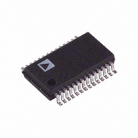
AD7564BRS Analog Devices Inc, AD7564BRS Datasheet - Page 2

AD7564BRS
Manufacturer Part Number
AD7564BRS
Description
IC DAC 12BIT LC2MOS QUAD 28-SSOP
Manufacturer
Analog Devices Inc
Datasheet
1.AD7564BRSZ.pdf
(16 pages)
Specifications of AD7564BRS
Mounting Type
Surface Mount
Rohs Status
RoHS non-compliant
Settling Time
500ns
Number Of Bits
12
Data Interface
Serial
Number Of Converters
4
Voltage Supply Source
Single Supply
Power Dissipation (max)
50µW
Operating Temperature
-40°C ~ 85°C
Package / Case
28-SSOP
Resolution (bits)
12bit
No. Of Pins
28
Peak Reflow Compatible (260 C)
No
Update Rate
1.8MSPS
No. Of Bits
12 Bit
Leaded Process Compatible
No
Interface Type
Serial
Lead Free Status / RoHS Status
Contains lead / RoHS non-compliant
Available stocks
Company
Part Number
Manufacturer
Quantity
Price
Part Number:
AD7564BRS
Manufacturer:
ADI/亚德诺
Quantity:
20 000
Part Number:
AD7564BRS-B
Manufacturer:
ADI/亚德诺
Quantity:
20 000
Company:
Part Number:
AD7564BRSZ
Manufacturer:
Maxim
Quantity:
456
Part Number:
AD7564BRSZ
Manufacturer:
ADI/亚德诺
Quantity:
20 000
Part Number:
AD7564BRSZ-REEL
Manufacturer:
ADI/亚德诺
Quantity:
20 000
AD7564–SPECIFICATIONS
Normal Mode
Parameter
ACCURACY
REFERENCE INPUT
DIGITAL INPUTS
DIGITAL OUTPUT (SDOUT)
POWER REQUIREMENTS
NOTES
1
2
Specifications subject to change without notice.
Temperature range is as follows: B Version: –40 C to +85 C.
Not production tested. Guaranteed by characterization at initial product release.
Resolution
Relative Accuracy
Differential Nonlinearity
Gain Error
Gain Temperature Coefficient
Output Leakage Current
Input Resistance
Ladder Resistance Mismatch
V
V
I
C
Output Low Voltage (V
Output High Voltage (V
V
Power Supply Rejection
I
INH
DD
INH
INL
DD
IN
+25 C
T
I
@ +25 C
T
OUT1
, Input Capacitance
Gain/ V
MIN
MIN
, Input Current
, Input Low Voltage
, Input High Voltage
Range
to T
to T
DD
MAX
MAX
(V
unless otherwise noted)
DD
2
OL
2
OH
= +4.75 V to +5.25 V; I
)
)
2
B Grade
12
2
5
10
50
6
13
2
2.4
0.8
10
0.4
4.0
4.75/5.25
–75
10
0.5
0.5
4
5
1
1
OUT1
A to I
Units
Bits
LSB max
LSB max
LSBs max
LSBs max
ppm FSR/ C typ
ppm FSR/ C max
nA max
nA max
k min
k max
% max
V min
V max
pF max
V max
V min
V min/V max
dB typ
A max
A max
OUT1
D = I
OUT2
–2–
A = I
OUT2
D = AGND = 0 V; V
Part Functions from 3.3 V to 5.25 V
Test Conditions/Comments
1 LSB = V
All Grades Guaranteed Monotonic Over Temperature
Typical Input Resistance = 9.5 k
Typically 0.6%
Load Circuit as in Figure 2.
V
At Input Levels of 0.8 V and 2.4 V, I
Typically 2 mA.
INH
= V
DD
REF
, V
/2
INL
REF
12
= +10 V; T
= 2.44 mV when V
= 0 V
A
= T
MIN
to T
DD
REF
MAX
is
,
= 10 V
REV. A


