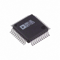
AD7836ASZ Analog Devices Inc, AD7836ASZ Datasheet - Page 9

AD7836ASZ
Manufacturer Part Number
AD7836ASZ
Description
IC DAC 14BIT QUAD LC2MOS 44MQFP
Manufacturer
Analog Devices Inc
Datasheet
1.AD7836ASZ.pdf
(12 pages)
Specifications of AD7836ASZ
Data Interface
Parallel
Settling Time
16µs
Number Of Bits
14
Number Of Converters
4
Voltage Supply Source
Analog and Digital, Dual ±
Power Dissipation (max)
460mW
Operating Temperature
-40°C ~ 85°C
Mounting Type
Surface Mount
Package / Case
44-MQFP, 44-PQFP
Resolution (bits)
14bit
Sampling Rate
62.5kSPS
Input Channel Type
Parallel
Supply Current
7mA
Digital Ic Case Style
QFP
No. Of Pins
44
Lead Free Status / RoHS Status
Lead free / RoHS Compliant
Available stocks
Company
Part Number
Manufacturer
Quantity
Price
Company:
Part Number:
AD7836ASZ
Manufacturer:
ADI
Quantity:
183
Company:
Part Number:
AD7836ASZ
Manufacturer:
Analog Devices Inc
Quantity:
10 000
Part Number:
AD7836ASZ
Manufacturer:
ADI/亚德诺
Quantity:
20 000
Power-On with CLR Low
The output stage of the AD7836 has been designed to allow
output stability during power-on. If CLR is kept low during
power-on, then just after power is applied to the AD7836, the
situation is as depicted in Figure 14. G
while G
V
G
parallel with the gain resistors of the output amplifier. The out-
put amplifier is connected as a unity gain buffer via G
DUTGND voltage is applied to the buffer input via G
amplifier’s output is thus at the same voltage as the DUTGND
pin. The output stage remains configured as in Figure 14 until
the voltage at V
now the output amplifier has enough headroom to handle sig-
nals at its input and has also had time to settle. The internal
power-on circuitry opens G
situation is shown in Figure 15. Now the output amplifier is
configured in its noise gain configuration via G
DUTGND voltage is still connected to the noninverting input
via G2 and this voltage appears at V
V
opening of G
via the configuration shown in Figure 15.
When CLR is taken back high, the output stage is configured as
shown in Figure 16. The internal control logic closes G
opens G
gain of two configuration. The voltage that appears on the Vout
pins is determined by the data present in the DAC registers. To
set all output voltages to the same known state, a write to
DATA REG E with the SEL pin high allows all DAC registers
to be updated with the same data.
REV. A
OUT
OUT
5
Figure 15. Output Stage with V
and a 6kΩ resistor. This thin-film resistor is connected in
is kept within a few hundred millivolts of DUTGND via
has been disconnected from the DUTGND pin by the
2
2
, G
DAC
DAC
. The output amplifier is connected in a noninverting
Figure 14. Output Stage with V
3
5
and G
but will track the voltage present at DUTGND
DD
G
G
G
G
and V
1
1
5
2
2
are closed.
R
R
SS
G
reaches approximately ± 10 V. By
3
G
DUTGND
DUTGND
4
4
and G
G
G
G
G
R
R
5
5
3
3
5
OUT
and closes G
6k
6k
DD
1
, G
.
> 10 V and CLR Low
G
G
6
6
4
and G
DD
4
< 10 V
and G
4
6
and G
are open
V
V
3
OUT
OUT
2
, and the
6
. The
1
. The
and
6
. This
–9–
Power-On with CLR High
If CLR is high on the application of power to the device, the
output stages of the AD7836 are configured as in Figure 17
while V
thereby connecting the output of the DAC to the input of its
output amplifier. G
open thus connecting the output amplifier as a unity gain
buffer. V
resistor until V
Figure 17. Output Stage Powering Up with CLR High
While V
When the supplies reach ± 10 V, the internal power on circuitry
opens G
stage as shown in Figure 18.
Figure 18. Output Stage Powering Up with CLR High
When V
Figure 16. Output Stage After CLR Is Taken High
DD
3
DD
DD
DAC
OUT
DAC
DAC
and G
/V
/V
/V
SS
SS
SS
is connected to DUTGND via G
DD
are less than ± 10 V. G
< ± 10 V
> ± 10 V
5
and closes G
G
G
G
and V
G
G
G
1
1
1
3
2
2
2
and G
R
R
R
SS
reach approximately ± 10 V.
G
DUTGND
5
G
DUTGND
G
DUTGND
4
4
4
are closed while G
4
G
G
G
G
G
G
R
R
and G
R
5
5
3
3
5
3
6k
6k
6k
1
6
is closed and G
configuring the output
G
G
G
6
6
6
5
4
AD7836
through a 6 kΩ
and G
V
V
V
OUT
OUT
OUT
2
6
is open
are


