ADDAC85D-CBI-V Analog Devices Inc, ADDAC85D-CBI-V Datasheet - Page 3
ADDAC85D-CBI-V
Manufacturer Part Number
ADDAC85D-CBI-V
Description
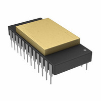
IC DAC 12BIT LOW COST 24-CDIP
Manufacturer
Analog Devices Inc
Datasheet
1.ADDAC80NZ-CBI-V.pdf
(16 pages)
Specifications of ADDAC85D-CBI-V
Rohs Status
RoHS non-compliant
Settling Time
2µs
Number Of Bits
12
Data Interface
Parallel
Number Of Converters
1
Voltage Supply Source
Dual ±
Power Dissipation (max)
300mW
Operating Temperature
0°C ~ 70°C
Mounting Type
Through Hole
Package / Case
24-CDIP (0.600", 15.24mm)
Available stocks
Company
Part Number
Manufacturer
Quantity
Price
Company:

Part Number:
ADDAC85D-CBI-V
Manufacturer:
a
Quantity:
32


Model
TEMPERATURE RANGE
NOTES
1
2
3
4
5
6
7
Specifications shown in boldface are tested on all production units at final electrical test. Results from those tests are used to calculate outgoing quality levels. All min
and max specifications are guaranteed, although only those shown in boldface are tested on all production units.
Specifications subject to change without notice.
Model
TECHNOLOGY
DIGITAL INPUT
TRANSFER CHARACTERISTICS
CONVERSION SPEED
Least Significant Bit.
Adjustable to zero with external trim potentiometer.
FSR means “Full Scale Range” and is 20 V for the ± 10 V range and 10 V for the ± 5 V range.
Gain and offset errors adjusted to zero at 25°C.
C
Maximum with no degradation of specification, must be a constant load.
A minimum of ± 12.3 V is required for a ± 10 V full scale output and ± 11.4 V is required for all other voltage ranges.
F
Specifications
Operating
Storage
Binary–CBI
BCD–CCD
Logic Levels (TTL Compatible)
ACCURACY
DRIFT (T
Voltage Model (V)
Current Model (I)
= 0, see Figure 3a.
V
V
I
I
Linearity Error @ 25°C
Differential Linearity Error @ 25°C
Gain Error
Offset Error
Temperature Range for Guaranteed
Monotonicity
Total Bipolar Drift, max (includes gain,
offset, and linearity drifts)
Total Error (T
Gain
Unipolar Offset
Bipolar Offset
Settling Time to ± 0.01% of FSR for
FSR Change (2 kΩ 500 pF load)
For LSB Change
Settling time to ± 0.01% of FSR for
FSR Change
IH
IL
IH
IL
CBI
CCD
T
CBI
CCD
T
Unipolar
Bipolar
Including Internal Reference
Excluding Internal Reference
with 10 kΩ Feedback
with 5 kΩ Feedback
Slew Rate
10 Ω to 100 Ω Load
for 1 kΩ
(V
(V
(Logic “0”)
(Logic “1”)
A
A
IL
IH
@ T
@ T
= 0.8 V)
= 5.5 V)
MIN
MIN
MIN
2
2
to T
to T
to T
MIN
5
MAX
MAX
to T
MAX
)
MAX
)
4
Min
0
–25
–25
Min
2.0
0
0
10
ADDAC80
ADDAC80
Hybrid
Typ
Typ
250
–100
± 1/4
± 1/8
± 1/4
± 1/2
± 1/4
± 0.1
± 0.05
± 0.08
± 0.06
± 15
± 5
± 1
± 5
5
3
1.5
15
300
1
Max
+70
+85
+125
Max
12
3
5.5
0.8
± 1/2
± 1/4
± 1/2
± 3/4
± 1/2
± 1
± 0.3
± 0.15
+70
± 20
± 0.15
± 0.10
± 30
± 7
± 3
± 10
Min
–25
–55
–65
Min
2.0
0
0
ADDAC85
ADDAC85
Hybrid
Typ
Typ
250
–100
± 1/4
± 1/2
± 1/2
± 0.1
± 0.05
± 1
5
3
1.5
20
300
1
Max
+85
+125
+150
Max
12
3
5.5
0.8
± 1/2
± 1/4
± 1/2
± 1
+70
± 20
± 10
± 10
ADDAC80/ADDAC85/ADDAC87
Min
–55
–55
–65
Min
2.0
0
–25
ADDAC87
ADDAC87
Hybrid
Typ
Typ
250
–100
± 1/2
± 1/2
± 1/2
± 0.1
± 0.05
± 1
5
3
1.5
20
300
1
Max
+125
+125
+150
Max
12
3
5.5
0.8
± 1/2
± 1/4
± 1/2
± 1
+85
± 20
± 10
± 10
Unit
°C
°C
°C
Unit
Bits
Digits
V
V
µA
µA
%FSR
%FSR
°C
ppm of FSR/°C
% of FSR
% of FSR
ppm of FSR/°C
ppm of FSR/°C
ppm of FSR/°C
ppm of FSR/°C
µs
µs
µs
V/µs
ns
µs
LSB
LSB
LSB
LSB
LSB
LSB
1
3
3
Related parts for ADDAC85D-CBI-V
Image
Part Number
Description
Manufacturer
Datasheet
Request
R

Part Number:
Description:
IC,D/A CONVERTER,SINGLE,12-BIT,BIPOLAR,DIP,24PIN
Manufacturer:
Analog Devices Inc

Part Number:
Description:
±1.7g Dual-Axis IMEMS Accelerometer Evaluation Board
Manufacturer:
Analog Devices Inc
Datasheet:
Part Number:
Description:
Inertial Sensor Evaluation System
Manufacturer:
Analog Devices Inc
Datasheet:
Part Number:
Description:
Manufacturer:
Analog Devices Inc
Datasheet:
Part Number:
Description:
Manufacturer:
Analog Devices Inc
Datasheet:
Part Number:
Description:
Manufacturer:
Analog Devices Inc
Datasheet:
Part Number:
Description:
Manufacturer:
Analog Devices Inc
Datasheet:
Part Number:
Description:
Manufacturer:
Analog Devices Inc
Datasheet:
Part Number:
Description:
Manufacturer:
Analog Devices Inc
Datasheet:
Part Number:
Description:
Manufacturer:
Analog Devices Inc
Datasheet:
Part Number:
Description:
Manufacturer:
Analog Devices Inc
Datasheet:
Part Number:
Description:
Manufacturer:
Analog Devices Inc
Datasheet:
Part Number:
Description:
Manufacturer:
Analog Devices Inc
Datasheet: