ADDAC85D-CBI-V Analog Devices Inc, ADDAC85D-CBI-V Datasheet - Page 8
ADDAC85D-CBI-V
Manufacturer Part Number
ADDAC85D-CBI-V
Description
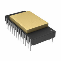
IC DAC 12BIT LOW COST 24-CDIP
Manufacturer
Analog Devices Inc
Datasheet
1.ADDAC80NZ-CBI-V.pdf
(16 pages)
Specifications of ADDAC85D-CBI-V
Rohs Status
RoHS non-compliant
Settling Time
2µs
Number Of Bits
12
Data Interface
Parallel
Number Of Converters
1
Voltage Supply Source
Dual ±
Power Dissipation (max)
300mW
Operating Temperature
0°C ~ 70°C
Mounting Type
Through Hole
Package / Case
24-CDIP (0.600", 15.24mm)
Available stocks
Company
Part Number
Manufacturer
Quantity
Price
Company:

Part Number:
ADDAC85D-CBI-V
Manufacturer:
a
Quantity:
32


ADDAC80/ADDAC85/ADDAC87
ACCURACY
Accuracy error of a D/A converter is the difference between the
analog output that is expected when a given digital code is
applied and the output that is actually measured with that code
applied to the converter. Accuracy error can be caused by gain
error, zero error, linearity error, or any combination of the three.
Of these three specifications, the linearity error specification is
the most important since it cannot be corrected. Linearity error
is specified over its entire temperature range. This means that
the analog output will not vary by more than its maximum
specification, from an ideal straight line drawn between the
end points (inputs all “1”s and all “0”s) over the specified
temperature range.
Differential linearity error of a D/A converter is the deviation
from an ideal 1 LSB voltage change from one adjacent output
state to the next. A differential linearity error specification of
± 1/2 LSB means that the output voltage step sizes can range
from 1/2 LSB to 1 1/2 LSB when the input changes from one
adjacent input state to the next.
DRIFT
Gain Drift
A measure of the change in the full scale range output over
temperature expressed in parts per million of full scale range
per °C (ppm of FSR/°C). Gain drift is established by: 1) testing
the end point differences for each ADDAC80 model at the
lowest operating temperature, 25°C and the highest operating
temperature; 2) calculating the gain error with respect to the
25°C value and; 3) dividing by the temperature change.
Offset Drift
A measure of the actual change in output with all “1”s on the
input over the specified temperature range. The maximum
change in offset is referenced to the offset at 25°C and is
divided by the temperature range. This drift is expressed in
parts per million of full scale range per °C (ppm of FSR/°C).
SETTLING TIME
Settling time for each model is the total time (including slew
time) required for the output to settle within an error band
around its final value after a change in input.
Voltage Output Models
Three settling times are specified to 0.01% of full scale range
(FSR); two for maximum full scale range changes of 20 V, 10 V
and one for a 1 LSB change. The 1 LSB change is measured at
the major carry (0 1 1 1 . . . 1 1 to 1 0 0 0 . . . 0 0), the point at
which the worst case settling time occurs. The settling time
characteristic depends on the compensation capacitor selected,
the optimum value is 25 pF as shown in Figure 3a.
Current Output Models
Two settling times are specified to ± 0.01% of FSR. Each is given
for current models connected with two different resistive loads:
10 Ω to 100 Ω and 1000 Ω to 1875 Ω. Internal resistors are provided
for connecting nominal load resistances of approximately 1000 Ω
to 1800 Ω for output voltage ranges of ±1 V and 0 V to –2 V.
POWER SUPPLY SENSITIVITY
Power supply sensitivity is a measure of the effect of a power
supply change on the D/A converter output. It is defined as a
percent of FSR per percent of change in either the positive or
negative supplies about the nominal power supply voltages.
REFERENCE SUPPLY
All models are supplied with an internal 6.3 V reference voltage
supply. This voltage (Pin 24) is accurate to ± 1% and must be
connected to the Reference Input (Pin 16) for specified opera-
tion. This reference may also be used externally with external
current drain limited to 2.5 mA. An external buffer amplifier is
recommended if this reference is to be used to drive other sys-
tem components. Otherwise, variations in the load driven by the
reference will result in gain variations. All gain adjustments
should be made under constant load conditions.
ANALYZING DEVICE ACCURACY OVER THE
TEMPERATURE RANGE
For the purposes of temperature drift analysis, the major device
components are shown in Figure 4. The reference element and
buffer amplifier drifts are combined to give the total reference
temperature coefficient. The input reference current to the
DAC, I
show the same drift rate as the reference voltage. The DAC
output current, I
codes, is designed to track I
these currents over temperature, it will contribute to the gain
T.C. The bipolar offset resistor, R
R
system drift errors. The input offset voltage drift of the output
amplifier, OA, also contributes a small error.
GAIN
, also have temperature coefficients that contribute to
REF
1–12
, is developed from the internal reference and will
DATA
IN
100
0%
90
10
JUNCTION
SUMMING
DAC
10V
>1mV
, which is a function of the digital input
20
18
25pF
C
V
REF
5V
5V
OUT
F
; if there is a slight mismatch in
15
BP
, and gain setting resistor,
100pF
500ns
2k
TEKTRONIX
7A13
HP6216A
10V
Related parts for ADDAC85D-CBI-V
Image
Part Number
Description
Manufacturer
Datasheet
Request
R

Part Number:
Description:
IC,D/A CONVERTER,SINGLE,12-BIT,BIPOLAR,DIP,24PIN
Manufacturer:
Analog Devices Inc

Part Number:
Description:
±1.7g Dual-Axis IMEMS Accelerometer Evaluation Board
Manufacturer:
Analog Devices Inc
Datasheet:
Part Number:
Description:
Inertial Sensor Evaluation System
Manufacturer:
Analog Devices Inc
Datasheet:
Part Number:
Description:
Manufacturer:
Analog Devices Inc
Datasheet:
Part Number:
Description:
Manufacturer:
Analog Devices Inc
Datasheet:
Part Number:
Description:
Manufacturer:
Analog Devices Inc
Datasheet:
Part Number:
Description:
Manufacturer:
Analog Devices Inc
Datasheet:
Part Number:
Description:
Manufacturer:
Analog Devices Inc
Datasheet:
Part Number:
Description:
Manufacturer:
Analog Devices Inc
Datasheet:
Part Number:
Description:
Manufacturer:
Analog Devices Inc
Datasheet:
Part Number:
Description:
Manufacturer:
Analog Devices Inc
Datasheet:
Part Number:
Description:
Manufacturer:
Analog Devices Inc
Datasheet:
Part Number:
Description:
Manufacturer:
Analog Devices Inc
Datasheet: