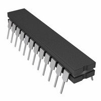
AD660SQ Analog Devices Inc, AD660SQ Datasheet - Page 11

AD660SQ
Manufacturer Part Number
AD660SQ
Description
IC DAC 16BIT MONO W/VREF 24-CDIP
Manufacturer
Analog Devices Inc
Series
DACPORT®r
Datasheet
1.AD660ARZ.pdf
(20 pages)
Specifications of AD660SQ
Rohs Status
RoHS non-compliant
Settling Time
6µs
Number Of Bits
16
Data Interface
Serial
Number Of Converters
1
Voltage Supply Source
Analog and Digital, Dual ±
Power Dissipation (max)
625mW
Operating Temperature
-55°C ~ 125°C
Mounting Type
Through Hole
Package / Case
24-CDIP (0.300", 7.62mm)
Available stocks
Company
Part Number
Manufacturer
Quantity
Price
BIPOLAR CONFIGURATION
The circuit shown in Figure 10 provides a bipolar output voltage
from −10.000000 V to +9.999694 V with positive full scale occur-
ring with all bits on. As in the unipolar mode, Resistor R1 and
Resistor R2 can be eliminated altogether to provide AD660 bipolar
operation without any external components. Eliminating these
resistors increases the gain error by 0.50% of FSR in bipolar mode.
Gain offset and bipolar zero errors can be adjusted to zero using
the circuit shown in Figure 11 as follows:
1.
2.
3.
LDAC
50Ω
HBE
SER
CLR
R1
Offset adjust.
Turn off all bits. Adjust the trimmer, R2, to give 10.000000 V
output.
Gain adjust.
Turn all bits on and adjust R1 to give a reading of 9.999694 V.
Bipolar zero adjust (optional).
In applications where an accurate zero output is required, set
the MSB on, all other bits off, and readjust R2 for 0 V output.
CLEAR SELECT
16
17
18
19
23
REF IN
LBE/
15
REF OUT
CONTROL
Figure 10. ±10 V Bipolar Voltage Output
LOGIC
10kΩ
50Ω
10V REF
R2
24
CS
14
DB0/
DB8/
SIN
12
–V
16-BIT LATCH
16-BIT LATCH
1
EE
DB1/DB9/
16-BIT DAC
DATADIR
11
+V
2
CC
DB15
DB7/
5
+V
AD660
3
10.05kΩ
LL
10kΩ
DGND
4
13
22
21
20
V
SPAN/
BIPOLAR
OFFSET
S
AGND
OUT
OUT
OUTPUT
Rev. B | Page 11 of 20
Note that using external resistors introduces a small temperature
drift component beyond that inherent in the AD660. The inter-
nal resistors are trimmed to ratio-match and temperature-track
other resistors on-chip, even though their absolute tolerances are
±20% and absolute temperature coefficients are approximately
−50 ppm/°C. In the case that external resistors are used, the
temperature coefficient mismatch between internal and external
resistors, multiplied by the sensitivity of the circuit to variations
in the external resistor value, is the resultant additional tempera-
ture drift.
INTERNAL/EXTERNAL REFERENCE USE
The AD660 has an internal low noise buried Zener diode
reference that is trimmed for absolute accuracy and temperature
coefficient. This reference is buffered and optimized for use in a
high speed DAC and gives long-term stability equal or superior to
the best discrete Zener diode references. The performance of
the AD660 is specified with the internal reference driving the
DAC and with the DAC alone (for use with a precision external
reference).
The internal reference has sufficient buffering to drive external
circuitry in addition to the reference currents required for the
DAC (typically 1 mA to REF IN and 1 mA to SPAN/BIPOLAR
OFFSET). A minimum of 2 mA is available for driving external
loads. The AD660 reference output should be buffered with an
external op amp if it is required to supply more than 4 mA total
current. The reference is tested and guaranteed to ±0.2%
maximum error.
Figure 11. ±10 V Bipolar Voltage Output with Gain and Offset Adjustment
LDAC
50Ω
HBE
SER
CLR
R1
CLEAR SELECT
16
17
18
19
23
REF IN
LBE/
15
REF OUT
CONTROL
LOGIC
10kΩ
10V REF
24
CS
14
100Ω
DB0/
DB8/
R2
SIN
12
–V
16-BIT LATCH
16-BIT LATCH
1
EE
DB1/DB9/
16-BIT DAC
DATADIR
11
+V
2
DB15
CC
DB7/
5
+V
AD660
10.05kΩ
3
LL
10kΩ
DGND
4
13
22
21
20
V
AD660
S
SPAN/
BIPOLAR
OFFSET
AGND
OUT
OUT
OUTPUT


