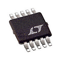
LTC4212CMSTR Linear Technology, LTC4212CMSTR Datasheet - Page 11

LTC4212CMSTR
Manufacturer Part Number
LTC4212CMSTR
Description
Manufacturer
Linear Technology
Datasheet
1.LTC4212CMSTR.pdf
(24 pages)
Specifications of LTC4212CMSTR
Linear Misc Type
Positive Low Voltage
Family Name
LTC4212
Package Type
MSOP
Operating Supply Voltage (min)
2.5V
Operating Supply Voltage (max)
16.5V
Operating Temperature (min)
0C
Operating Temperature (max)
70C
Operating Temperature Classification
Commercial
Product Depth (mm)
3mm
Product Height (mm)
0.86mm
Product Length (mm)
3mm
Mounting
Surface Mount
Pin Count
10
Lead Free Status / Rohs Status
Not Compliant
OPERATIO
set C
the specific applications.
Table 1. t
Power-Up Timeout Circuit
The power-up timeout circuit has two functions. During
power-up, it trips the circuit breaker if the DC/DC convert-
ers on the board do not power-up and do not enter
regulation on time. After normal power-up, it is configured
to trip the circuit breaker if any of the converters exit
regulation for longer than a programmable delay. Once the
circuit breaker is tripped, the LTC4212 is latched off and
the board is disconnected from the system supply. The ON
pin must be taken low for 120 s to reset the circuit breaker
and then high to reconnect the board to the backplane
supply.
The power-up timeout circuit uses three pins: PGI or
power good input pin, PGT or power good timer pin and
PGF or power good filter pin. It is enabled at the end of the
second system timing cycle, provided that the FAULT pin
is high. Prior to being enabled or if FAULT is low, the PGT
and PGF pins are pulled to GND by internal N-channel
FETs, M5 and M12 respectively. When enabled, the
power-up timeout circuit starts the power good timer,
which generates a time-out period before the PGI pin is
sampled.
TIMER
TIMER
= 10nF and adjust its value accordingly to suit
0.0033 F
0.0047 F
0.0068 F
0.0082 F
0.015 F
0.022 F
0.033 F
0.047 F
0.068 F
0.082 F
C
0.01 F
0.15 F
0.22 F
0.33 F
0.1 F
TIMER
vs C
TIMER
U
13.6ms
20.4ms
29.0ms
42.0ms
50.7ms
61.8ms
92.7ms
136ms
204ms
t
2.0ms
2.9ms
4.2ms
5.1ms
6.2ms
9.3ms
TIMER
Power Good Timer
The timer consists of COMP9, M8-M12, two 5 A current
sources and 0.65V and 0.95V threshold voltages for
COMP9.
The PGI pin is normally connected to the RST output pin
or comparator outputs of an external supply monitor IC or
to the PGOOD pin of a DC/DC converter and drives a
comparator, COMP8 which has a threshold voltage of
1.236V and 28mV of hysterisis. The RST and PGOOD pins
are typically open drain pins and require an external pull-
up resistor. The upper end of the resistor must be con-
nected to a voltage greater than the upper threshold of the
PGI comparator (1.236V).
A capacitor, C
programs the time-out period generated by the power
good timer according to Equation 3. Table 2 shows the
power good time-out periods for a list of standard capaci-
tor values.
Two 5 A current sources are switched in and out to charge
and discharge C
cycles.
Table 2. t
t
TIMEOUT
TIMEOUT
0.022 F
0.033 F
0.047 F
0.068 F
0.082 F
= 1.81 • C
0.01 F
0.22 F
0.33 F
0.47 F
0.68 F
0.82 F
3.3nF
4.7nF
6.8nF
8.2nF
0.1 F
C
1 F
PGT
PGT
vs C
PGT
, connected from the PGT pin to ground
PGT
between 0.65V and 0.95V for 14
PGT
t
1230ms
1480ms
1810ms
5.97ms
8.51ms
12.3ms
14.8ms
18.1ms
39.8ms
59.7ms
85.1ms
TIMEOUT
123ms
148ms
181ms
136ms
398ms
851ms
LTC4212
11
4212f
(3)


