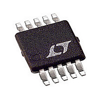
LTC4212CMSTR Linear Technology, LTC4212CMSTR Datasheet - Page 3

LTC4212CMSTR
Manufacturer Part Number
LTC4212CMSTR
Description
Manufacturer
Linear Technology
Datasheet
1.LTC4212CMSTR.pdf
(24 pages)
Specifications of LTC4212CMSTR
Linear Misc Type
Positive Low Voltage
Family Name
LTC4212
Package Type
MSOP
Operating Supply Voltage (min)
2.5V
Operating Supply Voltage (max)
16.5V
Operating Temperature (min)
0C
Operating Temperature (max)
70C
Operating Temperature Classification
Commercial
Product Depth (mm)
3mm
Product Height (mm)
0.86mm
Product Length (mm)
3mm
Mounting
Surface Mount
Pin Count
10
Lead Free Status / Rohs Status
Not Compliant
ELECTRICAL CHARACTERISTICS
temperature range, otherwise specifications are T
SYMBOL
V
V
V
V
V
I
I
I
V
V
V
V
t
t
t
t
t
t
t
t
Note 1: Absolute Maximum Ratings are those values beyond which the life
of a device may be impaired.
Note 2: All current into device pins are positive; all current out of device
pins are negative; all voltages are referenced to ground unless otherwise
specified.
PGT
PGF
TMR
TO
FAULTLO
FAULTVG
FAULTFC
FAULTSC
EXTFAULT
RESET
OFF
PGFHI
PGFHST
PGTHI
PGTLO
PGT V
TMR
FAULT
FAULTHST
OLFAULT
PARAMETER
Power Good Glitch Filter High Threshold
Power Good Glitch Filter Hysterisis
Power Good Timer High Threshold
Power Good Timer Low Threshold
Power Good Timer Delta Threshold
Power Good Timer Pin Current
Power Good Glitch Filter Pin Current
TIMER Current
TIMER Threshold
FAULT Threshold
FAULT Threshold Hysteresis
Output Low Voltage
Power Good Time-Out
Power Good Input Low at Time-Out to
GATE Discharging
Valid Power Good Glitch to GATE
Discharging
FAST COMP Trip to GATE Discharging
SLOW COMP Trip to GATE Discharging V
FAULT Low to GATE Discharging
Circuit Breaker Reset Delay Time
Turn-Off Time
CONDITIONS
(Note 4)
Power Good Timer On, C
Power Good Timer On, C
Power Good Timer Off, PGT = 1.5V
Power Good Timer Off, PGF = 1.5V
Timer On, V
Timer Off, TIMER = 1.5V
TIMER Low to High
TIMER High to Low
I
C
End of 14th PGT Cycle
V
ON Low to GATE Off
Power Good Glitch Filter On, C
Latched Off Threshold, FAULT High to Low
PGF > 1.26V
V
ON Low to FAULT High
FAULT
PGT
CB
CB
FAULT
A
= 0mV to 200mV Step
= 0mV to 100mV Step
= 25 C. V
=10nF, PGT = 0.1V to FAULT Low
= 1.6mA
= 5V to 0V
TIMER
The
CC
= 1V
= 5V, unless otherwise noted. (Note 2)
denotes specifications which apply over the full operating
PGT
PGT
Note 3: An internal clamp limits the GATE pin to a minimum of 10V above
V
a lower GATE pin voltage is desired, use an external zener diode. The GATE
capacitance must be < 0.15 F at maximum V
Note 4: Guaranteed by design and not tested in production.
CC
Charging, PGT = 0.65V
Discharging, PGT = 0.95V
. Driving this pin to voltages beyond the clamp may damage the part. If
PGF
Charging
– 5.61
– 5.61
0.928
0.640
0.283
– 2.5
MIN
1.20
4.63
1.20
0.15
1.20
16.3
10
1
CC
.
1.236
0.952
0.657
0.295
1.236
0.200
1.236
18.16
– 5.1
0.14
TYP
-5.1
500
120
5.2
1.5
– 2
40
50
18
10
5
5
5
1
3
LTC4212
– 4.59
– 4.49
0.976
0.680
0.304
MAX
1.26
5.77
– 1.5
1.26
0.40
1.26
700
250
0.4
20
30
5
UNITS
3
4212f
mV
mA
mA
mA
mV
ms
ns
V
V
V
V
V
V
V
A
A
A
A
V
s
s
s
s
s
s


