MAX5511ETC+ Maxim Integrated Products, MAX5511ETC+ Datasheet - Page 3
MAX5511ETC+
Manufacturer Part Number
MAX5511ETC+
Description
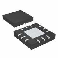
IC DAC 8BIT VOUT 12-TQFN-EP
Manufacturer
Maxim Integrated Products
Datasheet
1.MAX5510ETC.pdf
(18 pages)
Specifications of MAX5511ETC+
Settling Time
660µs
Number Of Bits
8
Data Interface
Serial
Number Of Converters
1
Voltage Supply Source
Single Supply
Operating Temperature
-40°C ~ 85°C
Mounting Type
Surface Mount
Package / Case
12-TQFN Exposed Pad
Resolution
8 bit
Interface Type
Serial (SPI)
Supply Voltage (max)
5.5 V
Supply Voltage (min)
1.8 V
Mounting Style
SMD/SMT
Supply Current
0.007 mA
Voltage Reference
Internal
Lead Free Status / RoHS Status
Lead free / RoHS Compliant
Power Dissipation (max)
-
Lead Free Status / Rohs Status
Lead free / RoHS Compliant


ELECTRICAL CHARACTERISTICS (continued)
(V
Power-Supply Rejection Ratio
REFERENCE INPUT (MAX5510)
Reference-Input Voltage Range
Reference-Input Impedance
REFERENCE OUTPUT (MAX5511)
Initial Accuracy
Output-Voltage Temperature
Coefficient
Line Regulation
Load Regulation
Output Noise Voltage
Short-Circuit Current (Note 6)
Capacitive Load Stability Range
Thermal Hysteresis
Reference Power-Up Time (from
Shutdown)
Long-Term Stability
DAC OUTPUT (OUT)
Capacitive Driving Capability
Short-Circuit Current (Note 6)
DD
= +1.8V to +5.5V, OUT unloaded, T
PARAMETER
_______________________________________________________________________________________
+1.8V to +5.5V, Ultra-Low-Power, 8-Bit,
SYMBOL
V
V
R
V
TEMPCO
REFOUT
PSRR
REFIN
REFIN
C
A
L
= T
MIN
1.8V ≤ V
Normal operation
In shutdown
No external load, V
No external load, V
No external load, V
No external load, V
T
V
0 ≤ I
V
0 ≤ I
V
-150µA ≤ I
0.1Hz to 10Hz, V
10Hz to 10kHz, V
0.1Hz to 10Hz, V
10Hz to 10kHz, V
V
V
(Note 7)
(Note 8)
REFOUT unloaded, V
REFOUT unloaded, V
V
shorted to GND, source current
V
V
V
shorted to GND, source current
V
V
to T
A
REFOUT
REF
REF
DD
DD
DD
DD
DD
DD
DD
DD
= -40°C to +85°C (Note 4)
, sink current
, sink current
REFOUT
REFOUT
MAX
= 5V
= 1.8V
= 5V, V
= 5V, V
= 1.8V, V
= 1.8V, V
= 1.2V
= 3.9V
DD
, unless otherwise noted. Typical values are at T
< V
REFOUT
≤ 5.5V
OUT
OUT
≤ 1mA, sourcing, V
≤ 8mA, sourcing, V
DD
OUT
OUT
CONDITIONS
- 200mV (Note 5)
REFOUT
REFOUT
set to full scale, OUT
set to 0V, OUT shorted to
REFOUT
REFOUT
≤ 0, sinking
set to full scale, OUT
set to 0V, OUT shorted to
DD
DD
DD
DD
DD
DD
= 1.8V
= 2.5V
= 3V
= 5V
= 5V
= 1.8V
= 3.9V
= 1.2V
Voltage-Output DACs
= 3.9V
= 1.2V
DD
DD
= 1.8V,
= 5V,
1.197
1.913
2.391
3.828
MIN
4.1
0
0 to 10
A
1.214
1.940
2.425
3.885
1000
TYP
150
600
450
200
200
2.5
0.3
0.3
0.2
5.4
4.4
85
12
50
30
14
= +25°C.)
2
1.231
1.967
2.459
3.941
MAX
V
200
30
65
65
14
14
DD
2
2
ppm/°C
UNITS
µV/µA
µV
ppm/
1khrs
µV/V
ppm
MΩ
GΩ
mA
ms
mA
dB
pF
nF
V
V
P-P
3
Related parts for MAX5511ETC+
Image
Part Number
Description
Manufacturer
Datasheet
Request
R

Part Number:
Description:
MAX7528KCWPMaxim Integrated Products [CMOS Dual 8-Bit Buffered Multiplying DACs]
Manufacturer:
Maxim Integrated Products
Datasheet:
Part Number:
Description:
Single +5V, fully integrated, 1.25Gbps laser diode driver.
Manufacturer:
Maxim Integrated Products
Datasheet:
Part Number:
Description:
Single +5V, fully integrated, 155Mbps laser diode driver.
Manufacturer:
Maxim Integrated Products
Datasheet:
Part Number:
Description:
VRD11/VRD10, K8 Rev F 2/3/4-Phase PWM Controllers with Integrated Dual MOSFET Drivers
Manufacturer:
Maxim Integrated Products
Datasheet:
Part Number:
Description:
Highly Integrated Level 2 SMBus Battery Chargers
Manufacturer:
Maxim Integrated Products
Datasheet:
Part Number:
Description:
Current Monitor and Accumulator with Integrated Sense Resistor; ; Temperature Range: -40°C to +85°C
Manufacturer:
Maxim Integrated Products
Part Number:
Description:
TSSOP 14/A�/RS-485 Transceivers with Integrated 100O/120O Termination Resis
Manufacturer:
Maxim Integrated Products
Part Number:
Description:
TSSOP 14/A�/RS-485 Transceivers with Integrated 100O/120O Termination Resis
Manufacturer:
Maxim Integrated Products
Part Number:
Description:
QFN 16/A�/AC-DC and DC-DC Peak-Current-Mode Converters with Integrated Step
Manufacturer:
Maxim Integrated Products
Part Number:
Description:
TDFN/A/65V, 1A, 600KHZ, SYNCHRONOUS STEP-DOWN REGULATOR WITH INTEGRATED SWI
Manufacturer:
Maxim Integrated Products
Part Number:
Description:
Integrated Temperature Controller f
Manufacturer:
Maxim Integrated Products
Part Number:
Description:
SOT23-6/I�/45MHz to 650MHz, Integrated IF VCOs with Differential Output
Manufacturer:
Maxim Integrated Products
Part Number:
Description:
SOT23-6/I�/45MHz to 650MHz, Integrated IF VCOs with Differential Output
Manufacturer:
Maxim Integrated Products
Part Number:
Description:
EVALUATION KIT/2.4GHZ TO 2.5GHZ 802.11G/B RF TRANSCEIVER WITH INTEGRATED PA
Manufacturer:
Maxim Integrated Products
Part Number:
Description:
QFN/E/DUAL PCIE/SATA HIGH SPEED SWITCH WITH INTEGRATED BIAS RESISTOR
Manufacturer:
Maxim Integrated Products
Datasheet: