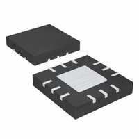
MAX5511ETC+ Maxim Integrated Products, MAX5511ETC+ Datasheet - Page 5

MAX5511ETC+
Manufacturer Part Number
MAX5511ETC+
Description
IC DAC 8BIT VOUT 12-TQFN-EP
Manufacturer
Maxim Integrated Products
Datasheet
1.MAX5510ETC.pdf
(18 pages)
Specifications of MAX5511ETC+
Settling Time
660µs
Number Of Bits
8
Data Interface
Serial
Number Of Converters
1
Voltage Supply Source
Single Supply
Operating Temperature
-40°C ~ 85°C
Mounting Type
Surface Mount
Package / Case
12-TQFN Exposed Pad
Resolution
8 bit
Interface Type
Serial (SPI)
Supply Voltage (max)
5.5 V
Supply Voltage (min)
1.8 V
Mounting Style
SMD/SMT
Supply Current
0.007 mA
Voltage Reference
Internal
Lead Free Status / RoHS Status
Lead free / RoHS Compliant
Power Dissipation (max)
-
Lead Free Status / Rohs Status
Lead free / RoHS Compliant
TIMING CHARACTERISTICS
(V
TIMING CHARACTERISTICS
(V
Note 1: Linearity is tested within codes 6 to 255.
Note 2: Offset is tested at code 6.
Note 3: Gain is tested at code 250. FB is connected to OUT.
Note 4: Guaranteed by design. Not production tested.
Note 5: V
Note 6: Outputs can be shorted to V
Note 7: Optimal noise performance is at 2nF load capacitance.
Note 8: Thermal hysteresis is defined as the change in the initial +25°C output voltage after cycling the device from T
Note 9: All digital inputs at V
Note 10: Load = 10kΩ in parallel with 100pF, V
TIMING CHARACTERISTICS (V
Serial Clock Frequency
DIN to SCLK Rise Setup Time
DIN to SCLK Rise Hold Time
SCLK Pulse-Width High
SCLK Pulse-Width Low
CS Pulse-Width High
SCLK Rise to CS Rise Hold Time
CS Fall to SCLK Rise Setup Time
SCLK Fall to CS Fall Setup
CS Rise to SCK Rise Hold Time
TIMING CHARACTERISTICS (V
Serial Clock Frequency
DIN to SCLK Rise Setup Time
DIN to SCLK Rise Hold Time
SCLK Pulse-Width High
SCLK Pulse-Width Low
CS Pulse-Width High
SCLK Rise to CS Rise Hold Time
CS Fall to SCLK Rise Setup Time
SCLK Fall to CS Fall Setup
CS Rise to SCK Rise Hold Time
DD
DD
= +4.5V to +5.5V, T
= +1.8V to +5.5V, T
DD
PARAMETER
PARAMETER
must be a minimum of 1.8V.
_______________________________________________________________________________________
A
A
+1.8V to +5.5V, Ultra-Low-Power, 8-Bit,
= T
= T
DD
MIN
MIN
or GND.
DD
DD
to T
to T
DD
= 4.5V TO 5.5V)
= 1.8V TO 5.5V)
SYMBOL
MAX
SYMBOL
MAX
f
f
t
or GND indefinitely, provided that the package power dissipation is not exceeded.
t
t
SCLK
t
t
t
t
SCLK
t
t
CSW
t
t
t
CSO
CSW
t
t
CSH
CSS
t
t
CSO
CS1
t
t
CSH
CSS
CS1
DH
CH
DS
CL
DH
CH
DS
CL
, unless otherwise noted. Typical values are at T
, unless otherwise noted. Typical values are at T
DD
= 5V, V
REF
= 4.096V (MAX5510) or V
CONDITIONS
CONDITIONS
Voltage-Output DACs
REF
A
A
= 3.9V (MAX5511).
= +25°C.)
= +25°C.)
MIN
100
MIN
150
15
24
24
20
20
24
40
40
30
30
0
0
0
0
0
0
0
0
TYP
TYP
MAX
16.7
MAX
MAX
10
to T
UNITS
UNITS
MIN
MHz
MHz
ns
ns
ns
ns
ns
ns
ns
ns
ns
ns
ns
ns
ns
ns
ns
ns
ns
ns
.
5


