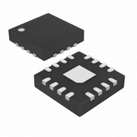
MAX5139GTE+T Maxim Integrated Products, MAX5139GTE+T Datasheet - Page 12

MAX5139GTE+T
Manufacturer Part Number
MAX5139GTE+T
Description
IC DAC V-OUT 12BIT 1CH 16-TQFN
Manufacturer
Maxim Integrated Products
Datasheet
1.MAX5139GTE.pdf
(17 pages)
Specifications of MAX5139GTE+T
Settling Time
5µs
Number Of Bits
12
Data Interface
DSP, I²C, MICROWIRE™, Parallel, QSPI™, SPI™
Number Of Converters
1
Voltage Supply Source
Analog and Digital
Operating Temperature
-40°C ~ 105°C
Mounting Type
Surface Mount
Package / Case
16-TQFN Exposed Pad
Lead Free Status / RoHS Status
Lead free / RoHS Compliant
Power Dissipation (max)
-
Low-Power, Single, 16-/12-Bit,
Buffered Voltage-Output DACs
Daisy chain multiple MAX5138/MAX5139 devices by
connecting the first device conventionally, then connect
its READY output to the CS of the following device.
Repeat for any other devices in the chain, and drive the
SCLK and DIN lines in parallel (Figure 5). When sending
commands to daisy-chained MAX5138/MAX5139s, the
devices are accessed serially starting with the first
device in the chain. The first 24 data bits are read by the
first device, the second 24 data bits are read by the sec-
ond device and so on (Figure 4). Figure 6 shows the
configuration when CS is not driven by the µC. These
devices can be daisy chained with other compatible
devices, such as the MAX5510 and the MAX5511.
To perform a daisy-chain write operation, drive CS low
and output the data serially to DIN. The propagation of
the READY signal then controls how the data is read by
each device. As the data propagates through the daisy
chain, each individual command in the chain is execut-
ed on the 24th falling clock edge following the falling
edge of the respective CS input. To update just one
device in a daisy chain, send the no-op command to
the other devices in the chain.
If READY is not required, write command 0x03 (power
control) and set READY_EN = 0 (see Table 1) to dis-
able the READY output.
The MAX5138/MAX5139 feature a software clear com-
mand (0x02). The software clear command acts as a
Figure 5. Daisy-Chain Configuration
12
______________________________________________________________________________________
μC
MOSI
SCK
I/O
Clear Command
DIN
SCLK
CS
SLAVE 1
READY
software POR, erasing the contents of all registers. The
output returns to the state determined by the M/Z input.
The MAX5138/MAX5139 feature a software-controlled
power-down mode. The internal reference and biasing
circuits power down to conserve power when powered
down. In power-down, the output disconnects from the
buffer and is grounded with an internal 80kΩ resistor.
The DAC register holds the retained code so that the
output is restored when powered up. The serial inter-
face remains active in power-down mode.
The MAX5138/MAX5139 feature an active-low LDAC
logic input that updates the output. Keep LDAC high
during normal operation (when the device is controlled
only through the serial interface). Drive LDAC low to
update the DAC output with data from the input register.
Figure 7 shows the LDAC timing with respect to OUT.
Holding LDAC low causes the input register to become
transparent and data written to the DAC register to
immediately update the DAC output. A software com-
mand can also activate the LDAC operation. To activate
LDAC by software, set control word 0x01 to load the
DAC, and all other data bits to don’t care. See Table 1
for the data format. This operation updates the DAC out-
put if it is flagged with a 1. If the DAC output is flagged
with a 0 it remains unchanged.
DIN
SCLK
CS
SLAVE 2
READY
Load DAC ( LDAC ) Input
Power-Down Mode
DIN
SCLK
CS
SLAVE 3
READY


