LM4854LD National Semiconductor, LM4854LD Datasheet
LM4854LD
Specifications of LM4854LD
Available stocks


Related parts for LM4854LD

LM4854LD Summary of contents
Page 1
... The LM4854 is available in the very space-efficient 12-lead micro SMD, exposed-DAP LLP for higher power applica- tions, and TSSOP packages. Note 1: An LM4854LD that has been properly mounted to a circuit board will deliver 1.7W (typ) into a 4Ω load. Key Specifications j LLP BTL output power (R = 3.2Ω ...
Page 2
Typical Application FIGURE 1. Typical Audio Amplifier Application Circuit (Pin out shown for the 12-pin large bump micro SMD IBL package. Consult the "Connection Diagrams" for the LLP or MT package pin out.) www.national.com 2 20038201 ...
Page 3
Connection Diagrams LM4854IBL Pin Designation 20038202 Top View (Bump-side down) Order Number LM4854IBL See NS Package Number BLA12BAB Micro SMD Marking 20038203 Top View X - Date Code T - Die Traceability G - Boomer Family 54 - LM4854IBL Pin ...
Page 4
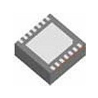
... Connection Diagrams Top View Order Number LM4854LD See NS Package Number LDA14A Top View Order Number LM4854MT See NS Package Number MTC14 www.national.com 20038204 Bottom Line - Part Number 20038205 Bottom 2 lines - Part Number 4 200382A5 Top View U - Fab Code Z - Plant Code XY - Date Code TT - Die Tracebility ...
Page 5
... Absolute Maximum Ratings 3) If Military/Aerospace specified devices are required, please contact the National Semiconductor Sales Office/ Distributors for availability and specifications. Supply Voltage Storage Temperature Input Voltage Power Dissipation(Note 4) ESD Susceptibility (Note 5) All pins except Pin C3 (IBL), Pin11 (LD/MT) Pin C3 (IBL), Pin 11 (LD/MT) ...
Page 6
... A Conditions THD = 1% (max 1kHz (Note12 3.2Ω (LM4854LD 4Ω (LM4854LD 8Ω L THD = 10% (max 1kHz (Note12 3.2Ω (LM4854LD 4Ω (LM4854LD 8Ω L 20Hz ≤ f ≤ 20kHz 4Ω 1.0W (LM4854LD 8Ω 400mW 1kHz 4Ω 1.5W (LM4854LD 8Ω 50mW 1kHz 1.0µF IN BYPASS P = 900mW 8Ω ...
Page 7
... 8Ω L THD = 10% (max 1kHz (Note11 4Ω (LM4854LD 8Ω L 20Hz ≤ f ≤ 20kHz 4Ω 800mW (LM4854LD 8Ω 150mW 1kHz 4Ω 500mW (LM4854LD 8Ω 150mW 1kHz 1.0µF IN BYPASS P = 900mW 8Ω 3.0V) (Continued 25˚C. A LM4854 (Limits) Typical Limit (Note 8) (Notes 9, ...
Page 8
... Note 10: Datasheet minimum and maximum specification limits are guaranteed by design, test, or statistical analysis. Note 11: Output power is measured at the amplifier’s package pins. Note 12: When driving 4Ω loads and operating supply, the LM4854LD must be mounted to a circuit board that has a minimum of 2.5in2 of exposed, uninterrupted copper area connected to the LLP package’s exposed DAP. ...
Page 9
... The filter’s cutoff frequency 1/2π Refer to the Application Information section sets the closed-loop gain. i 200382D8 200382C0 1/2π and R create ’s value. i THD+N vs Frequency 200382D9 LM4854LD 4Ω (BTL 400mW OUT THD+N vs Frequency 200382B8 16Ω (SE 50mW OUT www.national.com and ...
Page 10
... Typical Performance Characteristics THD+N vs Frequency 32Ω (SE 50mW OUT THD+N vs Frequency 8Ω (BTL 150mW OUT www.national.com (Continued) THD+N vs Frequency 200382B9 THD+N vs Frequency 200382B7 200382E0 LM4854LD = 4Ω (BTL 150mW OUT 200382B5 = 16Ω (SE 30mW OUT ...
Page 11
... L at (from top to bottom at 0.2W) 20kHz, 20Hz, 1kHz (Continued) THD+N vs Output Power 200382B6 (from top to bottom at 200mW) 20kHZ, 20Hz, 1kHz THD+N vs Output Power 200382C6 (from top to bottom at 30mW) 20kHz, 20Hz, 1kHz 11 200382E1 LM4854LD = 5V 4Ω (BTL), L 200382C4 = 5V 16Ω (SE), L www.national.com ...
Page 12
... (from top to bottom at 0.02W) 20kHz, 20Hz, 1kHz www.national.com (Continued) THD+N vs Output Power 200382C5 (from top to bottom at 200mW) 20kHz, 20Hz, 1kHz THD+N vs Output Power 200382C3 (from top to bottom at 20mW) 20kHz, 20Hz, 1kHz 12 200382E2 LM4854LD = 3V 4Ω (BTL), L 200382C1 = 3V 16Ω (SE), L ...
Page 13
... Power Supply Voltage R = 16Ω (BTL 1kHz (from top to bottom at 4V): 10% THD+N, 1% THD+N (Continued) vs Power Supply Voltage 200382C2 R = 8Ω (BTL (from top to bottom at 4V) 10% THD+N, 1% THD+N PSRR vs Frequency 200382A7 Output Power 200382A8 = 1kHz, IN 200382E3 LM4854LD = 5V 4Ω (BTL 10Ω SOURCE www.national.com ...
Page 14
... Typical Performance Characteristics PSRR vs Frequency 8Ω (BTL 10Ω SOURCE PSRR vs Frequency 32Ω (SE 10Ω SOURCE www.national.com (Continued) PSRR vs Frequency 200382B4 PSRR vs Frequency 200382B3 200382B2 = 16Ω (SE 10Ω SOURCE 200382E4 LM4854LD = 4Ω (BTL 10Ω SOURCE ...
Page 15
Typical Performance Characteristics PSRR vs Frequency 8Ω (BTL 10Ω SOURCE PSRR vs Frequency 32Ω (SE 10Ω SOURCE (Continued) PSRR vs Frequency 200382B1 ...
Page 16
... Amplifier Power Dissipation vs Load Power Dissipation LM4854IBL/MT (from top to bottom at 0.04W 16Ω (SE 32Ω (SE both channels driven and loaded Power Dissipation Derating Curves LM4854LD 8Ω (BTL (from top to bottom at 120˚C): 2 4in copper plane heatsink area 2 1in copper plane heatsink area www ...
Page 17
Typical Performance Characteristics Power Dissipation Derating Curve LM4854MT 5V 8Ω (BTL 1kHz L IN Output Power vs Load Resistance LM4854IBL/MT, BTL Load, (from top to bottom at 12Ω): V = 5V, THD+N = ...
Page 18
Typical Performance Characteristics Channel-to-Channel Crosstalk vs Frequency 16Ω (SE Left channel driven, right channel measured B = Right channel driven, left channel measured Channel-to-Channel Crosstalk vs Frequency V = 3V, R ...
Page 19
Application Information the amplifier that drives the headphone jack’s sleeve. If this current exceeds 500mA , the amplifier is shutdown, pro- PK FIGURE 2. Typical Audio Amplifier Application Circuit EXPOSED-DAP MOUNTING CONSIDERATIONS The LM4854’s exposed-DAP (die attach paddle) package (LD) ...
Page 20
Application Information PCB LAYOUT AND SUPPLY REGULATION CONSIDERATIONS FOR DRIVING 3Ω AND 4Ω LOADS Power dissipated by a load is a function of the voltage swing across the load and the load’s impedance. As load imped- ance decreases, load dissipation ...
Page 21
Application Information power, higher ambient temperatures are allowed as output power or duty cycle decreases. If the result of Equation (3) is greater than that of Equation (4), then decrease the supply voltage, increase the load impedance, or reduce the ...
Page 22
Application Information FIGURE 3. Headphone Circuit Figure 4 shows an optional resistor connected between the amplifier output that drives the headphone jack sleeve and ground. This resistor provides a ground path that supressed power supply hum. This hum may occur ...
Page 23
Application Information OPTIMIZING CLICK AND POP REDUCTION PERFOR- MANCE The LM4854 contains circuitry that eliminates turn-on and shutdown transients ("clicks and pops") and transients that could occur when switching between BTL speakers and single-ended headphones. For this discussion, turn-on re- ...
Page 24
Application Information The product of the desired high frequency cutoff (100kHz in this example) and the differential gain AVD, determines the upper passband response limit. With AVD = 3 and fH = 100kHz, the closed-loop gain bandwidth product (GBWP) is ...
Page 25
Demonstration Board Layout (Continued) FIGURE 9. Recommended MM PC Board Layout: Bottom_Side Layout FIGURE 10. Recommended MT PC Board Layout: Component-Side SilkScreen FIGURE 11. Recommended MT PC Board Layout: Component-Side Layout FIGURE 12. Recommended MT PC Board Layout: Bottom-Side Layout ...
Page 26
Demonstration Board Layout www.national.com (Continued) FIGURE 15. Recommended LD PC Board Layout: Upper Inner-Layer Layout FIGURE 16. Recommended LD PC Board Layout: Lower Inner-Layer Layout FIGURE 17. Recommended LD PC Board Layout: Bottom-Side Layout 26 20038231 20038232 20038233 ...
Page 27
Physical Dimensions inches (millimeters) unless otherwise noted TSSOP Package Order Number LM4854MT NS Package Number MTC14 27 www.national.com ...
Page 28
... Physical Dimensions www.national.com inches (millimeters) unless otherwise noted (Continued) 14-Lead LLP Package Order Number LM4854LD NS Package Number LDA14A 28 ...
Page 29
... NATIONAL’S PRODUCTS ARE NOT AUTHORIZED FOR USE AS CRITICAL COMPONENTS IN LIFE SUPPORT DEVICES OR SYSTEMS WITHOUT THE EXPRESS WRITTEN APPROVAL OF THE PRESIDENT AND GENERAL COUNSEL OF NATIONAL SEMICONDUCTOR CORPORATION. As used herein: 1. Life support devices or systems are devices or systems which, (a) are intended for surgical implant ...