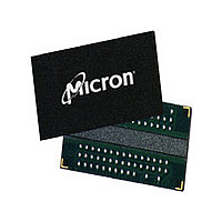
MT47H32M16HR-25E IT:F TR Micron Technology Inc, MT47H32M16HR-25E IT:F TR Datasheet - Page 12

MT47H32M16HR-25E IT:F TR
Manufacturer Part Number
MT47H32M16HR-25E IT:F TR
Description
Manufacturer
Micron Technology Inc
Type
DDR2 SDRAMr
Datasheet
1.MT47H32M16HR-25E_ITF_TR.pdf
(131 pages)
Specifications of MT47H32M16HR-25E IT:F TR
Organization
32Mx16
Density
512Mb
Address Bus
15b
Access Time (max)
400ps
Maximum Clock Rate
800MHz
Operating Supply Voltage (typ)
1.8V
Package Type
FBGA
Operating Temp Range
-40C to 85C
Operating Supply Voltage (max)
1.9V
Operating Supply Voltage (min)
1.7V
Supply Current
295mA
Pin Count
84
Mounting
Surface Mount
Operating Temperature Classification
Industrial
Lead Free Status / Rohs Status
Compliant
- Current page: 12 of 131
- Download datasheet (10Mb)
Figure 4: 64 Meg x 8 Functional Block Diagram
Figure 5: 32 Meg x 16 Functional Block Diagram
PDF: 09005aef82f1e6e2
512MbDDR2.pdf - Rev. Q 10/10 EN
BA0, BA1
BA0, BA1
A0–A12,
A0–A13,
RAS#
CAS#
WE#
ODT
RAS#
CAS#
CKE
CK#
ODT
WE#
CS#
CKE
CK#
CS#
CK
CK
16
15
Address
register
Address
register
registers
registers
Control
Mode
Mode
logic
Control
Logic
16
15
counter
Refresh
counter
Refresh
14
10
13
10
2
14
2
13
2
address
Row-
MUX
address
2
Row-
MUX
control
Column-
counter/
address
Bank
logic
latch
14
Column-
counter/
control
address
13
Bank
logic
latch
latch and
decoder
address
Bank 0
row-
latch and
Address
decoder
Bank 1
Bank 0
Bank 2
row-
Bank 1
Bank 3
8
2
Bank 2
Bank 3
16,384
8
2
8,192
DM mask logic
(16,384 x 256 x 32)
I/O gating
Sense amplifiers
DM mask logic
(8,192 x 256 x 64)
Sense amplifiers
Column
decoder
8,192
I/O gating
Memory
(x32)
Column
decoder
256
Bank 0
16,384
Bank 0
Memory
array
Bank 1
Bank 1
array
(x64)
Bank 2
256
Bank 2
Bank 3
Bank 3
internal
CK, CK#
COL0, COL1
32
12
Internal
CK, CK#
COL0, COL1
64
32
32
64
Read
latch
64
CK out
drivers
Write
FIFO
CK in
and
Read
CK out
latch
drivers
Write
CK in
FIFO
and
8
8
8
8
Micron Technology, Inc. reserves the right to change products or specifications without notice.
COL0, COL1
Mask
Data
MUX
32
4
16
16
16
16
Mask
Data
generator
64
COL0, COL1
8
512Mb: x4, x8, x16 DDR2 SDRAM
1
1
1
1
8
8
8
8
DQS
registers
MUX
Input
generator
Data
2
2
2
2
16
16
16
16
registers
8
DQS
Input
Data
1
1
1
1
8
8
8
8
DQS, DQS#
16
2
1
8
2
2
2
16
16
16
16
Functional Block Diagrams
CK, CK#
UDQS, UDQS#
LDQS, LDQS#
DRVRS
2
DLL
RCVRS
2
16
CK, CK#
4
DRVRS
2
DLL
4
RCVRS
sw1 sw2
sw1 sw2
sw1 sw2
sw1 sw2
R1
R1
R1
R1
R1
R1
© 2004 Micron Technology, Inc. All rights reserved.
sw1 sw2
sw1 sw2
sw1 sw2
sw1 sw2
R1
R1
R1
R1
R1
R1
ODT control
ODT control
R2
R2
R2
R2
R2
R2
VssQ
R2
R2
R2
R2
R2
R2
VssQ
sw3
sw3
sw3
sw3
sw3
sw3
R3
R3
R3
R3
R3
R3
sw3
sw3
R3
R3
R3
R3
R3
R3
VddQ
VddQ
DQ0–DQ15
UDM, LDM
UDQS, UDQS#
LDQS, LDQS#
RDQS
DM
DQ0–DQ7
DQS, DQS#
RDQS#
Related parts for MT47H32M16HR-25E IT:F TR
Image
Part Number
Description
Manufacturer
Datasheet
Request
R

Part Number:
Description:
IC DDR2 SDRAM 512MBIT 84FBGA
Manufacturer:
Micron Technology Inc
Datasheet:

Part Number:
Description:
IC DDR2 SDRAM 512MBIT 3NS 84FBGA
Manufacturer:
Micron Technology Inc
Datasheet:

Part Number:
Description:
32MX16 DDR2 SDRAM PLASTIC IND TEMP PBF FBGA 1.8V
Manufacturer:
Micron Technology Inc
Datasheet:

Part Number:
Description:
DRAM Chip DDR2 SDRAM 512M-Bit 32Mx16 1.8V 84-Pin FBGA T/R
Manufacturer:
Micron Technology Inc
Datasheet:

Part Number:
Description:
Manufacturer:
Micron Technology Inc
Datasheet:

Part Number:
Description:
Manufacturer:
Micron Technology Inc
Datasheet:

Part Number:
Description:
Manufacturer:
Micron Technology Inc
Datasheet:

Part Number:
Description:
Manufacturer:
Micron Technology Inc
Datasheet:

Part Number:
Description:
MICMT47H32M16HR-3_IT:F 32MBX16 DDR2
Manufacturer:
Micron Technology Inc
Datasheet:

Part Number:
Description:
Manufacturer:
Micron Technology Inc
Datasheet:

Part Number:
Description:
Manufacturer:
Micron Technology Inc
Datasheet:

Part Number:
Description:
32MX16 DDR2 SDRAM PLASTIC IND TEMP PBF FBGA 1.8V
Manufacturer:
Micron Technology Inc

Part Number:
Description:
IC DDR2 SDRAM 512MBIT 84FBGA
Manufacturer:
Micron Technology Inc
Datasheet:

Part Number:
Description:
Manufacturer:
Micron Technology Inc
Datasheet:

Part Number:
Description:
Manufacturer:
Micron Technology Inc
Datasheet:


