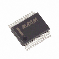
MAX503CAG+T Maxim Integrated Products, MAX503CAG+T Datasheet

MAX503CAG+T
Specifications of MAX503CAG+T
Related parts for MAX503CAG+T
MAX503CAG+T Summary of contents
Page 1
... D6/S0 D2 D8/D0 D4 D7/S1 D9/D1 D3 ________________________________________________________________ Maxim Integrated Products Call toll free 1-800-998-8800 for free samples or literature. 5V, Low-Power, Parallel-Input, Voltage-Output, 10-Bit DAC ____________________________Features Buffered Voltage Output Internal 2.048V Voltage Reference Operates from Single 5V or Dual ±5V Supplies Low Power Consumption: 250µA Operating Current 40µ ...
Page 2
Low-Power, Parallel-Input, Voltage-Output, 10-Bit DAC ABSOLUTE MAXIMUM RATINGS V to DGND and V to AGND ................................-0.3V, + DGND and V to AGND .................................-6V, +0. ............................................................... -0.3V, +12V DD SS AGND ...
Page 3
ELECTRICAL CHARACTERISTICS—Single +5V Supply (continued 5V 0V, AGND = DGND = REFGND = 0V, REFIN = 2.048V (external), RFB = ROFS = VOUT 10kΩ 100pF ...
Page 4
Low-Power, Parallel-Input, Voltage-Output, 10-Bit DAC ELECTRICAL CHARACTERISTICS—Dual ±5V Supplies ( -5V, AGND = DGND = REFGND = 0V, REFIN = 2.048V (external), RFB = ROFS = VOUT 10kΩ ...
Page 5
Operating Characteristics (Single +5V supply, unity gain, code = all 1s, T OUTPUT SINK CAPABILITY vs. OUTPUT PULL-DOWN VOLTAGE 0.2 0.4 0.6 0.8 1.0 OUTPUT PULL-DOWN VOLTAGE (V) REFERENCE ...
Page 6
Low-Power, Parallel-Input, Voltage-Output, 10-Bit DAC ____________________________Typical Operating Characteristics (continued) (Single +5V supply, unity gain, code = all 1s, T SUPPLY CURRENT vs. REFIN 250 REFGND = AGND 200 150 100 REFGND = EXTERNAL REFERENCE 0 0 ...
Page 7
Description PIN NAME 1 D7 input when input when and Always set S1 to 0 input when ...
Page 8
Low-Power, Parallel-Input, Voltage-Output, 10-Bit DAC ________________Detailed Description The MAX503 consists of a parallel-input logic interface, a 10-bit R-2R ladder, a reference, and an op amp. The Functional Diagram shows the control lines and signal flow through the input data ...
Page 9
R REFOUT S TOTAL C S REFERENCE NOISE C REFOUT TEK 7A22 300 SINGLE POLE ROLLOFF 250 C = 3.3 F REFOUT 200 150 100 REFOUT 0 0 100 FREQUENCY (kHz) Figure 2. ...
Page 10
Low-Power, Parallel-Input, Voltage-Output, 10-Bit DAC 33 F REFGND 2N7002 AGND POWER-ON DGND RESET CLR CLR A0 CONTROL LDAC Figure 3. Low-Current Shutdown Mode Table 2. Input Latch Addressing CLR CS WR LDAC A0 A1 DATA UPDATED ...
Page 11
A0– DATA BITS (8-BIT BYTE OR 4-BIT NIBBLE) CLR t CLR LDAC NOTE: TIMING MEASUREMENT REFERENCE LEVEL IS Figure 4. MAX503 Write-Cycle Timing Diagram A small error voltage is added to the reference output by the reference current ...
Page 12
Low-Power, Parallel-Input, Voltage-Output, 10-Bit DAC D0–D3 DATA BUS D0–D3 FROM S0, S1, D0, D1 SYSTEM CLR RESET A0, A1 MC6800 DECODER R/W ADDRESS BUS A0, A1 A13–A15 A0–A15 Figure 5. 4-Bit µP Interface ...
Page 13
NBL & NBM NBH CS WR LDAC = 0 (DAC LATCH IS TRANSPARENT) Figure 8b. 8-Bit and 16-Bit µP Timing Sequence with LDAC = 0 + REFIN ROFS REFOUT 33µF MAX503 AGND RFB DGND VOUT REFGND V SS ...
Page 14
Low-Power, Parallel-Input, Voltage-Output, 10-Bit DAC Table 3. Unipolar Binary Code Table ( Output), Gain = 1 REFIN OUTPUT INPUT* 1111 1111 (V 11(00) REFIN 01(00) (V 1000 0000 REFIN 512 00(00) 1000 0000 (V ) REFIN 1024 ...
Page 15
REFIN ROFS REFOUT 33µF MAX503 RFB AGND DGND VOUT REFGND -5V Figure 11. Bipolar Configuration (-2.048V to +2.048V Output) __________Applications Information Single-Supply Linearity As with any amplifier, the MAX503’s output op amp off- set can be positive or negative. ...
Page 16
... Maxim cannot assume responsibility for use of any circuitry other than circuitry entirely embodied in a Maxim product. No circuit patent licenses are implied. Maxim reserves the right to change the circuitry and specifications without notice at any time. 16 __________________Maxim Integrated Products, 120 San Gabriel Drive, Sunnyvale, CA 94086 (408) 737-7600 © 1994 Maxim Integrated Products Printed USA is a registered trademark of Maxim Integrated Products ...


