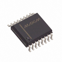
MAX532BCWE+T Maxim Integrated Products, MAX532BCWE+T Datasheet - Page 12

MAX532BCWE+T
Manufacturer Part Number
MAX532BCWE+T
Description
IC MDAC 12BIT DUAL SER 16-SOIC
Manufacturer
Maxim Integrated Products
Datasheet
1.MAX532ACPE.pdf
(16 pages)
Specifications of MAX532BCWE+T
Settling Time
2.5µs
Number Of Bits
12
Data Interface
Serial
Number Of Converters
2
Voltage Supply Source
Dual ±
Power Dissipation (max)
762mW
Operating Temperature
0°C ~ 70°C
Mounting Type
Surface Mount
Package / Case
16-SOIC (0.300", 7.5mm Width)
Lead Free Status / RoHS Status
Lead free / RoHS Compliant
The output amplifiers are stable with any combination
of resistive loads ≥ 2kΩ and capacitive loads ≤ 100pF.
They are internally compensated, and settle to ±0.01%
FSR (1/2LSB) in 2.5µs.
Figure 9 shows DACA connected for unipolar binary
operation. Similar connections apply for DACB. When
V
multiplication. Table 2 shows the codes for this circuit.
Figure 10 shows the MAX532 connected for bipolar
operation. The coding is offset binary, as shown in
Table 3. When V
four-quadrant multiplication. To maintain gain error
specifications, resistors R1, R2, and R3 should be ratio-
matched to 0.01%.
Dual, Serial-Input,
Voltage-Output, 12-Bit MDAC
Table 2. Unipolar Code Table
1LSB = V
Figure 10. Bipolar Operation
12
DAC Latch Contents
V
IN
IN
1111 1111 1111
1000 0000 0000
0000 0000 0001
0000 0000 0000
MSB
is an AC signal, the circuit performs two-quadrant
______________________________________________________________________________________
VREF_
IN
/4096
DGND
+12V to +15V
DAC_
V
LSB
DD
IN
is an AC signal, the circuit performs
AGND_
20k
R1
-V
-V
-V
0V
IN
IN
IN
-12V to -15V
Unipolar Configuration
MAX532
x (4095/4096)
x (2048/4096) = -1/2V
x (1/4096)
V
SS
Analog Output, V
VOUT_
RFB_
Output Amplifiers
Bipolar Operation
10k
R3
20k
OUT
R2
IN
V
OUT
For best system performance, use printed circuit boards
with separate analog and digital ground planes. Wire-
wrap boards are not recommended. The two ground
planes should be tied together at the low-impedance
power-supply source, as shown in Figure 11.
The board layout should ensure that digital and analog
signal lines are kept separate from each other as much
as possible. Do not run analog and digital lines parallel
to one another.
The output amplifiers are sensitive to high-frequency
noise in the V
these supplies to the analog ground plane with 0.1µF
and 10µF bypass capacitors. Minimize capacitor lead
lengths for best noise rejection.
Table 3. Bipolar Code Table
1LSB = V
Figure 11. Power-Supply Grounding
__________Applications Information
DAC Latch Contents
1111 1111 1111
1000 0000 0001
1000 0000 0000
0111 1111 1111
0000 0000 0000
MSB
+15V
V
IN
DD
/2048
Layout, Grounding, and Bypassing
-15V
V
SS
LSB
DD
ANALOG
AGNDA
SUPPLY
AGND
MAX532
and V
AGNDB
+V
+V
0V
-V
-V
SS
IN
IN
IN
IN
Analog Output, V
x (1/2048)
+ (2048/2048) = -V
x (2047/2048)
x (1/2048)
power supplies. Bypass
DGND
+5V
DIGITAL
SUPPLY
+5V
CIRCUITRY
DIGITAL
DGND
OUT
DGND
IN


